AI Boom Drives Demand for Ultra-Large Packaging as ASICs Expected to Shift from CoWoS to EMIB, Says TrendForce
November 25, 2025 -- TrendForce’s latest investigations reveal that the rapid expansion of AI and HPC is increasing the need for heterogeneous integration, positioning advanced packaging as a strategic priority. TSMC’s CoWoS platform is currently the leading solution in this area. However, as CSPs accelerate their in-house ASIC development to accommodate more complex functions, their packaging size requirements are growing substantially. As a result, some CSPs are contemplating a switch from TSMC’s CoWoS to Intel’s EMIB.
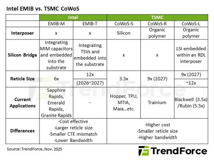
TrendForce notes that CoWoS connects compute logic, memory, and I/O dies via an interposer, which mounts them on a substrate. The technology has expanded to include CoWoS-S, CoWoS-R, and CoWoS-L. Demand has been strongly shifting toward CoWoS-L, which incorporates a silicon interposer into the package, as NVIDIA’s Blackwell platform approaches mass production in 2025. This trend is expected to continue with NVIDIA’s upcoming Rubin architecture, which will boast even larger reticle sizes.
The rise in AI/HPC demand has led to significant CoWoS bottlenecks, including capacity shortages, reticle size restrictions, and elevated manufacturing costs. TrendForce observes that most CoWoS capacity is already taken by NVIDIA GPUs, leaving other clients with limited options. Furthermore, the increasing demand for larger package sizes and US localization requirements are encouraging major North American CSPs, like Google and Meta, to collaborate with Intel on EMIB adoption.
TSMC leads with technology, but Intel counters with size and cost advantages
Intel’s EMIB provides several advantages over CoWoS. First, EMIB removes the necessity for a large, expensive interposer by integrating small silicon bridges directly into the substrate for die-to-die connections. This design simplifies the structure and enhances manufacturing yield. Second, EMIB minimizes thermal-expansion mismatches caused by materials with different CTEs, as only a small portion of the package contains silicon. This reduces the risk of warpage and boosts long-term reliability.
EMIB also enables larger effective reticle-size scaling: while CoWoS-S is limited to 3.3× and CoWoS-L is approximately 3.5× (projected to reach 9× by 2027), EMIB-M already supports 6× and is anticipated to achieve 8–12× by 2026–2027. Cost is another significant benefit—by eliminating the interposer, EMIB provides a more cost-effective solution for AI customers requiring very large packages.
However, EMIB has inherent limitations: the silicon bridge’s restricted area and routing density limit bandwidth, extend transmission distances, and cause slightly higher latency than CoWoS. Consequently, EMIB mainly attracts ASIC customers rather than GPU vendors, who demand very high bandwidth and very low latency.
According to TrendForce, since announcing the launch of its standalone Intel Foundry Services (IFS) unit in 2021, Intel has spent years developing EMIB advanced packaging technology. The company has successfully implemented this technology in its own server CPU platforms, including Sapphire Rapids and Granite Rapids. As Google plans to implement EMIB in its 2027 TPU v9 and Meta considers it for its MTIA accelerators, EMIB is set to significantly boost IFS's growth. Nonetheless, for the near future, CoWoS will continue to be the primary solution for high-bandwidth products from NVIDIA and AMD.
For more information on reports and market data from TrendForce’s Department of Semiconductor Research, please click here, or email the Sales Department at SR_MI@trendforce.com
Related Chiplet
- DPIQ Tx PICs
- IMDD Tx PICs
- Near-Packaged Optics (NPO) Chiplet Solution
- High Performance Droplet
- Interconnect Chiplet
Related News
- Alphawave Semi Launches Industry’s First 3nm UCIe IP with TSMC CoWoS Packaging
- CoWoS Drives Demand for Advanced Packaging Equipment; Sales Expected to Surpass 10% Growth in 2024
- Broadcom Bets on 3.5D Packaging Technology to Build Bigger AI Chips
- Sarcina Technology launches AI platform to enable cost-effective customizable AI packaging solutions
Latest News
- Adeia Enters into Multi-Year IP License Agreement with AMD
- STMicroelectronics enters high-volume production of its industry-leading silicon photonics platform to support AI infrastructure demand
- Vertical Compute raises €57M to solve the AI memory bottleneck with new high density memory
- Ayar Labs Closes $500M Series E, Accelerates Volume Production of Co-Packaged Optics
- NanoIC opens access to first-ever fine-pitch RDL and D2W hybrid bonding interconnect PDKs