NHanced Semiconductors President Robert Patti to Deliver Plenary Presentation on the Critical Role of Advanced Packaging at the 2026 Lithography Workshop
Patti will describe how advanced packaging technology is now the enabling factor for a renaissance in leading edge semiconductor design and manufacturing
SEDONA -- JUNE 19, 2026 – Robert Patti, President of NHanced Semiconductors, will deliver a plenary talk titled "Transitioning to Advanced Packaging Driven Semiconductors" at the 2026 Lithography Workshop to be held from June 22 – 25 at the Hilton Sedona Resort at Bell Rock in Sedona, AZ. The presentation will discuss the history of semiconductor packaging technology, the emerging toolsets and materials available, and what the future of advanced packaging holds for the semiconductor industry.
 Advanced packaging has deep roots in the semiconductor industry, dating back to multichip modules more than 40 years ago. Since that time, advanced packaging technologies have provided go-to solutions to a number of challenges for interconnects, thermal management, and 3D integration as the Moore’s Law benefits of scaling transistors have reached a point of diminishing returns. The next generation of processors, power supply modules, and memory devices will have advanced packaging technology as an integral component of their design and manufacturing.
“Advanced packaging is now driving the leading edge of semiconductor development, and it promises a renaissance for the electronics industry,” said Patti. “The ability to use next-generation i-line lithography tools, implement new technologies such as hybrid bonding, and fully integrate heterogeneous materials will enable gains in power and performance on a scale not seen in more than a decade. Advanced packaging allows the deconstruction and reaggregation of current SoCs for increased flexibility, reduced cost, and affordable innovation in semiconductor manufacturing.”
The 2026 Lithography Workshop will be held at the Hilton Sedona Resort at Bell Rock in Sedona, AZ from June 22 – 25. Now in its 29th iteration, the Workshop held its first meeting in Lake Placid, NY in 1981, and is dedicated to promoting the continuing evolution of lithography technology with a unique program of invited speakers designed to cover all aspects of advanced lithography developments. The Workshop program provides time for extensive questions and answers after each paper and poster session and during group meetings, which provides an opportunity for attendees to interact with leading experts in a broad range of disciplines. Student participation is encouraged.
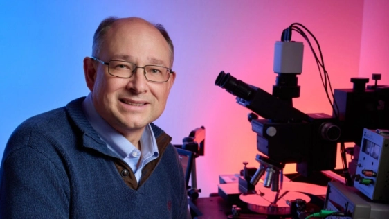
About Robert Patti
Bob is the president of NHanced Semiconductors, Inc. He has spearheaded the development and delivery of cutting-edge 3D and 2.5D integration technology for high energy physics, medicine, automotive, military, HPC, and other fields. He has managed hardware engineering teams in several organizations, including successful startups. Bob received the 2009 SEMI Award for North America for his pioneering work in 3D IC integration and the 2015 3DIncites Individual Achievement Award.
About NHanced Semiconductors, Inc.
Based in the US, NHanced Semiconductors is the world’s first pure-play advanced packaging foundry, specializing in leading-edge BEoL semiconductor technologies. Its capabilities include chiplets, 3D-ICs, silicon interposers, 2.5D, additive silicon manufacturing, photonics, microfluidics, and other innovative technologies. The foundry works with both standard and non-standard substrates, III‑V compound semiconductors, and many specialized materials.
Headquartered in Illinois, NHanced has a development and manufacturing facility near Research Triangle Park, NC, performing small volume manufacturing, in-house process development, and customer prototyping, and an advanced packaging and assembly facility in Odon, IN.
Related Chiplet
- eFPGA Chiplet
- DPIQ Tx PICs
- IMDD Tx PICs
- Near-Packaged Optics (NPO) Chiplet Solution
- High Performance Droplet
Related News
- NHanced Semiconductors President Robert Patti to Detail “Foundry 2.0” at SEMIEXPO Heartland
- EV Group Highlights Hybrid and Fusion Bonding, Layer Transfer and Maskless Lithography Technologies for Advanced Semiconductor Memory and Packaging at SEMICON Korea 2026
- EV Group Highlights Hybrid Bonding, Layer Transfer and Maskless Lithography Technologies for Heterogeneous Integration and Advanced Packaging at ECTC 2026
- Veeco Announces Over $35 Million in Advanced Packaging Lithography System Orders From IDM & OSAT Customers
Latest News
- TYLsemi Raises $43 Million to Launch First Full-Stack Chiplet Platform for Custom AI Silicon
- SILITH and UMC Achieve Mass Production Milestone for Silicon Photonics
- As AI Moves from Training to Inference, Optics Moves Closer to the Chip
- Arteris Announces Collaboration with IC-Link by imec to Accelerate Next-Gen AI and HPC Silicon
- Asahi Kasei Adds New Slitting Facility for SUNFORT™ to Meet Growing Demand for Advanced Semiconductor Packaging