Interconnect underdogs steering chiplet design bandwagon
By Majeed Ahmad , EDN (September 6, 2024)
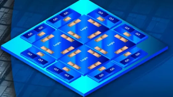
The chiplets movement is gaining steam, and it’s apparent from how this multi-die silicon premise is dominating the program of the AI Hardware and Edge AI Summit to be held in San Jose, California from 10 to 12 September 2024. The annual summit focuses on deep tech and machine learning ecosystems to explore advancements in artificial intelligence (AI) infrastructure and edge deployments.
At the event, Alphawave Semi’s CTO Tony Chan Carusone will deliver a speech on chiplets and connectivity while showing how AI has emerged as the primary catalyst for the rise of chiplet ecosystems. “The push for custom AI hardware is rapidly evolving, and I will examine how chiplets deliver the flexibility required to create energy-efficient systems-in-package designs that balance cost, power, and performance without starting from scratch,” he said while talking about his presentation at the event.
To read the full article, click here
Related Chiplet
- FlexGen Multi-Die Smart Network-on-Chip (NoC) IP
- Ncore Multi-Die Interconnect IP
- Integrated voltage regulator (IVR) chiplet
- High-performance connectivity chiplets
- eFPGA Chiplet
Related News
- Keysight Unveils 3D Interconnect Designer for Chiplet and 3DIC Advanced Package Designs
- Tenstorrent Selects Blue Cheetah Chiplet Interconnect IP For Its AI and RISC-V Solutions
- Baya Systems and Blue Cheetah Partner to Deliver Chiplet Interconnect Solutions
- Blue Cheetah Tapes Out Its High-Performance Chiplet Interconnect IP on Samsung Foundry SF4X
Latest News
- Racyics UCIe PHY IP for GlobalFoundries 22FDX reaches silicon
- EdgeCortix Unveils RAIDEN, a Scalable, Energy-Efficient AI Chiplet Platform Purpose-Built for Physical AI
- Coherent Launches PhotonLink™ Integrated Optics Platform for AI Infrastructure
- AT&S and Marvell Technology expand collaboration to support next-generation AI infrastructure
- SMART Photonics Partners with GlobalFoundries to Offer Industry’s First Open Access Foundry Service for Integrated Silicon and Indium Phosphide Photonics Products