Imec sets up R&D activities in Hokkaido to strengthen Japan's next-generation semiconductor and photonics ecosystem
New presence in Hokkaido will support collaborative R&D in photonics and advanced semiconductor technologies, bringing together academia, research institutes and industry
LEUVEN (Belgium) and TOKYO (Japan), November 16 2026 — Imec, a a global center for advanced semiconductor research and innovation, is expanding its activities in Hokkaido, Japan, with the backing of Japan's Ministry of Economy, Trade and Industry (METI) and in collaboration with Leading-edge Semiconductor Technology Center (LSTC), to support the development of next-generation semiconductor and photonics technologies. As part of this expansion, imec is building a local R&D team, reinforcing its long-term commitment to Japan's semiconductor ecosystem. The initiative will facilitate knowledge exchange and joint research activities between the two regions.
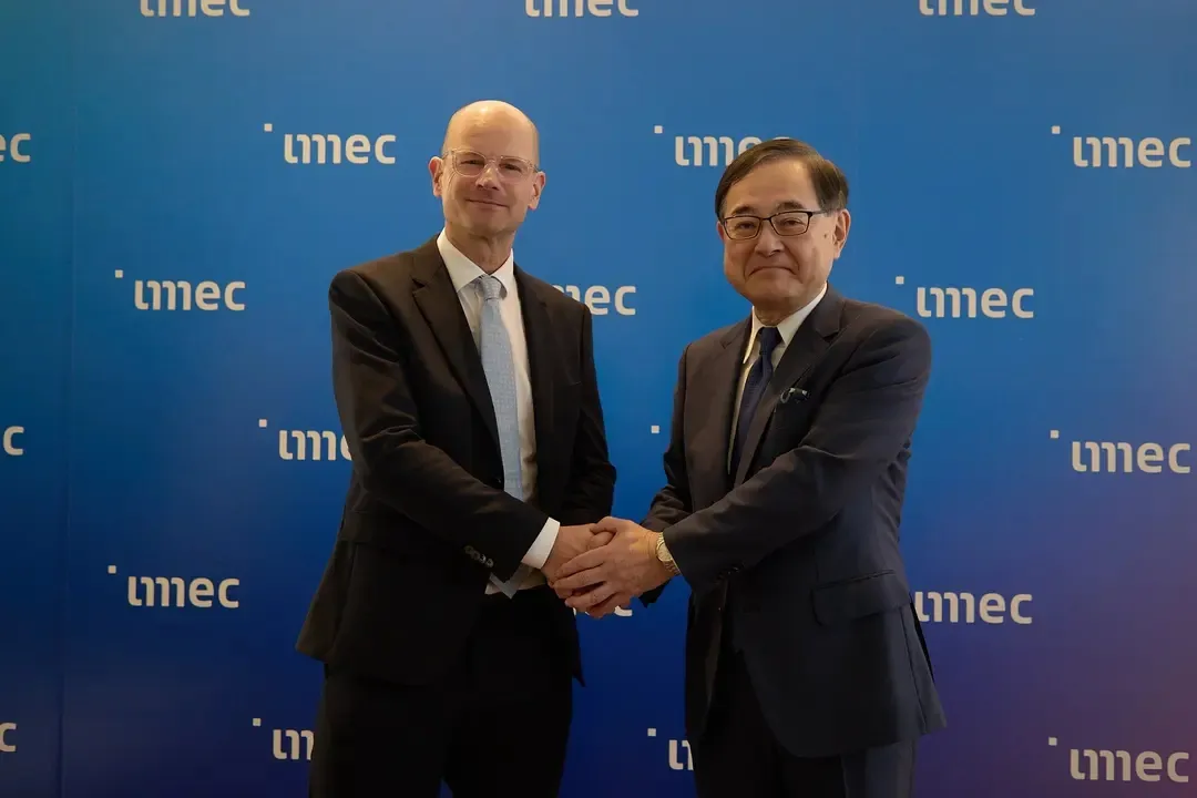
Patrick Vandenameele, CEO of imec and Koyohiro Houkin, President of Hokkaido University, announced at ITF Japan the establishment of imec Hokkaido.
Building on imec's growing collaborations across Japan and with Hokkaido as a rapidly emerging center for semiconductor innovation in Japan, the new presence reflects the increasing importance of photonics and co-packaged optics (CPO) technologies as the industry seeks more energy-efficient solutions to support future AI and high-performance computing systems. Fully integrated in imec’s global R&D activities, imec Japan’s Hokkaido R&D center will support national photonics-related research programs and foster collaboration between leading Japanese universities, research institutes and industry partners. To support these activities, imec intends to grow a local R&D team in Hokkaido to approximately 15 researchers and engineers over the next five years, while creating strong collaboration links between teams in Hokkaido and Leuven. The team will be based on the Hokkaido University campus in Sapporo, Hokkaido,forming imec's R&D base in Japan.
The Hokkaido-based team will work closely with organizations including Hokkaido University, Tohoku University, Yokohama National University, National Institute of Advanced Industrial Science and Technology (AIST) and Chitose Institute of Science and Technology to advance cutting-edge photonic integrated circuit (PIC) and electronic-photonic integrated circuit (EIC) technologies. These innovations are expected to play an important role in enabling future semiconductor systems and supporting the commercialization efforts of industry partners, including Rapidus Corporation, a Japanese advanced semiconductor manufacturer.
Patrick Vandenameele, CEO of imec: "Japan plays a vital role in the global semiconductor ecosystem, with world-class expertise spanning materials, equipment, manufacturing and research. Through our R&D activities in Hokkaido, we aim to contribute to Japan's ambitions in next-generation semiconductor and photonics technologies while further strengthening the connection between Japanese innovation and our global R&D ecosystem. By bringing together leading universities, research institutes and industry partners, we can accelerate innovation on common ground and help create the technologies that will power future generations of AI and digital infrastructure."
Kiyohiro Houkin, President of Hokkaido University: “After signing an LOI in November 2024, Hokkaido University and imec proposed joint projects for co-packaged optics R&D in semiconductors advanced packaging and medical AI use-case expansion, both of which kicked off this year. Training for our graduate students at imec has also begun. In the very year Hokkaido University celebrates its 150th anniversary, we are truly proud that our campus has become home to imec's first R&D base in Japan. Looking ahead, I hope this opportunity will accelerate the flow of talent and strengthen semiconductor partnership between Japan and Europe.”
The initiative complements imec's broader engagement with Japan's semiconductor ecosystem, where the organization has collaborated for many years with leading companies, universities and research institutes. By combining imec's expertise, world-class R&D infrastructure and global partner network with Japan's growing semiconductor ambitions, the collaboration aims to accelerate innovation and strengthen international cooperation in strategic technologies.
Related Press Releases
Development of Chiplet Packaging Technologies and Establishment of an Advanced Packaging R&D Center to Accelerate Photonics–Electric Convergence,
Research and Development Project of the Enhanced Infrastructures for Post-5G Information and Communication Systems/Development of Advanced Semiconductor Manufacturing Technology
https://www.meti.go.jp/policy/mono_info_service/joho/post5g/20260411.html (in Japanese)
https://www.lstc.jp/....LSTC_d6_press_20260409.pdf (in Japanese)
Imec and Hokkaido University endeavor to advance semiconductor innovation together
https://www.imec-int.com/en/press/imec-and-hokkaido-university-endeavor-advance-semiconductor-innovation-together
https://www.hokudai.ac.jp/news/2024/11/imec.html (in Japanese)
About imec
Imec is a global R&D center for advanced semiconductor technologies. Through its R&D collaborations, venturing activities and design & manufacturing capabilities, imec builds the hardware for tomorrow’s AI-driven era. The unique combination of its state-of-the-art R&D infrastructure, the largest semiconductor ecosystem and top talent of 6,500 employees, powers breakthroughs across a wide range of industries, including computing, connectivity, health, automotive, industry, consumer electronics, aerospace and security. Imec brings global technology leaders, start-ups, academia, and research institutions together on common ground to tackle technology challenges that no single company can solve alone.
Headquartered in Leuven, Belgium, imec has research facilities in Belgium, across Europe, the USA, Japan and the GCC region, and representation in Taiwan, Korea and India. In 2025, imec reported revenues of €1.2 billion.For more information, visit www.imec-int.com
The imec group holds a global trademark portfolio, including word marks and combined figurative registered and unregistered trademarks, across national, regional, and international territories. Its lawful use requires prior written consent of IMEC in compliance with the IMEC branding guidelines, which may be updated periodically. The latest version is available upon written request.
About Hokkaido University
Hokkaido University is one of Japan's leading national universities, originating from the Sapporo Agricultural College established in 1876. It hosts the largest number of schools among Japanese national universities, with 12 faculties and 21 graduate schools, covering almost all areas of humanities, social sciences, and natural sciences. With almost 2,000 faculty members, it boasts advanced research fields, including producing Nobel Prize laureates, offering an opportunity to learn from researchers with high levels of specialized knowledge in many fields. The student population exceeds 18,000, with about 2,000 international students from 96 countries. Hokkaido University also possesses extensive holdings, including experimental forests, and has been ranked 7th in THE Sustainability Impact Ratings 2026 for its contributions to the Sustainable Development Goals (SDGs).
Further information on Hokkaido University can be found at https://www.global.hokudai.ac.jp/.
Related Chiplet
- Optical Chiplet
- Reverse Gearbox Chiplet
- FlexGen Multi-Die Smart Network-on-Chip (NoC) IP
- Ncore Multi-Die Interconnect IP
- Integrated voltage regulator (IVR) chiplet
Related News
- Imec: Breaking Connectivity Wall with Silicon Photonics and More
- Arteris Joins Intel Foundry Accelerator Ecosystem Alliance Program to Support Advanced Semiconductor Designs
- Imec and TNO launch Holst Centre Photonics Lab
- Xscape Photonics and Tower Semiconductor Unveil the Industry’s First Optically Pumped On-Chip Multi-Wavelength Laser Platform for AI Datacenter Fabrics
Latest News
- Axelera AI Unveils Titania Dual-Chiplet Architecture for AI Inference
- Imec sets up R&D activities in Hokkaido to strengthen Japan's next-generation semiconductor and photonics ecosystem
- JEDEC® Announces Creation of JC-14.8 Subcommittee on System Level Reliability Testing (SLRT); Invites Industry Participation
- UCIe Consortium Advances from Chiplet Connectivity to System-Level Integration with UCIe 4.0 Specification
- Netherlands and Taiwan Launch Four Joint Photonics R&D Projects