How Advanced Packaging is Unleashing Possibilities for Edge AI
By Pax Wang, Division Director of Technology Development, UMC
EETimes | November 11, 2025
The rapid migration of AI from the cloud to edge devices is fueling explosive growth in edge AI. Sectors like automotive, PCs, robotics, smartphones and surveillance are accelerating adoption, with the number of edge AI devices projected to grow at 17% CAGR to more than 2 billion units by 2030.
Compared to cloud AI systems, which deliver up to 10,000 TOPS of computing power and require massive power budgets and high dollar investments, IC design for edge AI applications is completely different. Edge AI devices typically only require 1-50 TOPS with strict power (0.01-1W) and cost ($10-$1,000) constraints. This forces chip designers to address bandwidth, performance, form factor, thermal and cost challenges simultaneously.
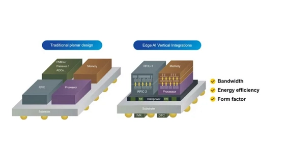
From planar to 3D: a turning point in edge AI design
Traditional planar chip architectures are reaching their limits as multimodal AI applications demand more bandwidth and compute resources, increasing chip area and power consumption. To address these challenges, the industry is increasingly embracing 3D vertical stacking, integrating processors, memory and other modules within a single package atop interposers.
The vertical stack approach shortens interconnects, which reduces signal loss and latency, lowers power use and enables more compact devices. The modular design of vertical stacking also improves yield and cost control.
To read the full article, click here
Related Chiplet
- eFPGA Chiplet
- DPIQ Tx PICs
- IMDD Tx PICs
- Near-Packaged Optics (NPO) Chiplet Solution
- High Performance Droplet
Related News
- Silicon Box Ships 100M Units, Proves Advanced Panel-Level Packaging Ready for AI, HPC era
- YES Selected to Deliver Full Portfolio of Advanced Packaging Tools for Glass Panel AI and HPC Applications by a Leading AI Infrastructure Supplier
- Applied Materials Introduces New Systems to Accelerate DRAM and Advanced Packaging for AI Chips
- TOPPAN to Install Pilot Line for Advanced Semiconductor Packaging at Ishikawa Plant
Latest News
- As AI Moves from Training to Inference, Optics Moves Closer to the Chip
- Arteris Announces Collaboration with IC-Link by imec to Accelerate Next-Gen AI and HPC Silicon
- Asahi Kasei Adds New Slitting Facility for SUNFORT™ to Meet Growing Demand for Advanced Semiconductor Packaging
- ACCM Introduces Celeritas SMC: A Production-Ready, Silicon-Matched Core for Advanced Packaging
- Socionext Addresses Datacenter Infrastructure Customer Demands for Advanced SoCs on TSMC A14 Technology