EV Group Addresses Critical Manufacturing Challenges for Next-Generation Co-Packaged Optics
Comprehensive portfolio of wafer bonding and nanoimprint lithography technologies enables customers and partners to develop scalable CPO architectures for AI-driven data centers and HPC applications
ST. FLORIAN, Austria, September 1, 2026—EV Group (EVG), a leading provider of innovative process solutions and expertise serving leading-edge and future semiconductor designs and chip integration schemes, today announced that it is actively engaged with customers and partners across the rapidly evolving co-packaged optics (CPO) ecosystem to support the needs of hyperscale data centers, AI infrastructure and high-performance computing (HPC) applications.
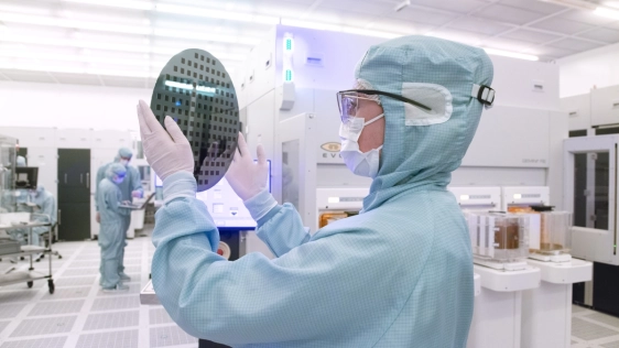 Drawing on decades of expertise in advanced packaging, heterogeneous integration and photonics manufacturing, EVG supports multiple stages of the CPO manufacturing value chain—from process development through high-volume manufacturing (HVM). EVG will showcase its latest CPO process advances during the presentation, “Enabling Scalable CPO Architectures Through Nanoimprint Lithography and Direct Bonding,” at the Heterogeneous Integration Global Summit, co-located with SEMICON Taiwan 2026, on Friday, September 4.
Co-Packaged Optics Drives New Manufacturing Requirements
Driven by exponential growth in AI workloads and hyperscale data center infrastructure, the semiconductor industry is increasingly adopting CPO architectures to overcome the bandwidth, latency, power efficiency and signal integrity limitations associated with conventional copper interconnects. CPO brings optical I/O closer to compute by combining photonic integrated circuits (PICs), lasers, and optical structures within the same package. Because these components are made from different materials with different physical and manufacturing properties, integrating them at increasingly higher densities requires new manufacturing approaches.
EVG addresses these challenges through its broad portfolio of wafer bonding, nanoimprint lithography and thin-wafer processing technologies, supported by the company’s NILPhotonics® Competence Center and Heterogeneous Integration Competence Center™ (HICC). These facilities enable customers and partners to develop, optimize and validate new product designs and manufacturing processes in a production-relevant environment before transferring them to HVM, helping accelerate time-to-market while reducing implementation risk.
“Co-packaged optics represents a major technology transition for AI hardware, but it also introduces significant integration challenges, requiring the integration of photonic and electronic components through advanced packaging technologies that demand comprehensive process expertise rather than just point solutions,” stated Dr. Bernd Dielacher, director of business development at EVG. “By combining decades of experience across these disciplines with close collaboration through our Competence Centers, EVG helps customers develop, optimize and validate complete manufacturing processes from early development through HVM, enabling the successful deployment of next-generation CPO architectures.”
Comprehensive Process Expertise for CPO Manufacturing
EVG’s process portfolio addresses numerous critical manufacturing requirements across the CPO ecosystem. Hybrid bonding enables low-parasitic integration of PICs and electronic integrated circuits (EICs) to support future bandwidth requirements, while fusion bonding enables heterogeneous integration of III-V semiconductor materials for laser fabrication as well as emerging modulation materials such as thin-film lithium niobate (TFLN) and barium titanate (BTO). Oxide-free room-temperature bonding ensures low-loss, optically transparent interfaces and integration of heat spreader materials such as diamond and silicon carbide (SiC) for effective heat transfer through interfaces.
Nanoimprint lithography provides a scalable manufacturing approach for grating couplers, vertical optical coupling elements and beam-shaping elements that facilitate efficient out-of-plane light coupling for chip-to-chip and chip-to-fiber optical interconnects, as well as wafer-level optics used in microLED lens packaging. Additional capabilities, including temporary bonding and debonding, support wafer thinning for laser diode fabrication and advanced packaging applications.
Looking beyond CPO, the industry is expected to transition towards optical I/O chiplet architectures and advanced 3D photonic-electronic integration, enabling even tighter co-integration of silicon photonics, CMOS electronics, and laser sources within highly scalable optical interconnect platforms. Building on its proven track record in semiconductor 3D/heterogenous integration, EVG is well positioned to support both today’s CPO implementations and future optical I/O architectures, extending established electronic integration concepts to the next generation of photonic-electronic systems.
Meet EVG at SEMICON Taiwan 2026
To speak with an EVG representative and learn more about the company’s industry-leading solutions for co-packaged optics and other critical technologies, visit EVG’s booth #L0310 during exhibition hours.
About EV Group (EVG)
EV Group (EVG) provides innovative process solutions and expertise that serve leading-edge and future semiconductor designs and chip integration schemes. The company’s vision of being the first in exploring new techniques and supporting next-generation applications of micro- and nanofabrication technologies enables customers to successfully commercialize new product ideas. EVG’s high-volume-manufacturing-ready products, which include wafer bonding, lithography, thin-wafer processing and metrology equipment, enable advances in semiconductor front-end scaling, 3D integration and advanced packaging, as well as in other electronics and photonics applications. More information about EVG is available at www.EVGroup.com.
Related Chiplet
- FlexGen Multi-Die Smart Network-on-Chip (NoC) IP
- Ncore Multi-Die Interconnect IP
- Integrated voltage regulator (IVR) chiplet
- High-performance connectivity chiplets
- eFPGA Chiplet
Related News
- EV Group Unveils Next-Generation EVG®120 Resist Processing System for High-Volume Manufacturing
- EV Group Advances 300-mm MEMS Manufacturing with Next-Generation GEMINI® Automated Production Wafer Bonding System
- Omni Design Technologies Advances 200G-Class Co-Packaged Optics IP Portfolio for Next-Generation AI Infrastructure
- EV Group Brings Revolutionary Layer Transfer Technology to High-Volume Manufacturing with EVG®850 NanoCleave™ System
Latest News
- Chiplets at the Edge: How Modular SoCs Redefine Performance Per Watt
- Visitech Launches 1-micron Maskless Photohead for Advanced Packaging
- GlobalFoundries reaches agreement to establish U.S.-based supply of silicon interposers for advanced AI packaging
- Applied Materials and Intel Collaborate to Accelerate Chipmaking Innovations for AI-Driven Computing
- BOS Semiconductors to Support MIRISE Technologies’ Automotive Chiplet R&D Project