ERS electronic Unveils Fully Automated 310 x 310mm Panel-Level Packaging System to Power AI and Chiplet Architectures
September 29, 2026 -- ERS electronic, the industry leader of thermal management solutions for semiconductor manufacturing, today announced its fully automated panel-level packaging (PLP) system for 310×310 mm substrates. The machine integrates temporary carrier bonding, debonding, and detaping into a single automated platform at 13 panels per hour, eliminating inter-tool transfers across three thermally critical process steps. The first unit has been delivered to a leading semiconductor manufacturer for integration into its panel production line.
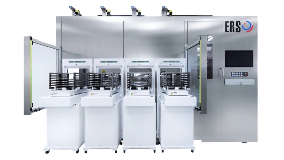 The machine is developed and manufactured at the company’s Advanced Packaging facility in Barbing, Germany. The facility combines ERS’s 55 years of thermal management expertise with more than 30 years of in-house machine-building capability, following ERS’s 2024 integration of a semiconductor specialist equipment engineering team.
ERS is considered an early adopter of panel-level packaging, as it shipped its first commercial panel-level tool to Fraunhofer IZM in Berlin in 2018. The 310×310 mm panel format is gaining traction across the industry because it improves substrate area utilisation significantly compared to 300 mm circular wafers. The panel-level packaging segment is projected to grow at a compound annual growth rate of over 40% over the next five years, according to Yole Group1. As dual-carrier bonding and debonding workflows become increasingly important for backside processing in 3D IC, HBM and 2.5D IC packaging, ERS’s integrated platform addresses these requirements in a single automated system.
In dual-carrier processes, bonding and debonding typically requires separate machines, often located at different points on the fab floor. Moving panels between them introduces handling steps, transit time, and the risk of substrate damage. ERS’s machine consolidates all three process steps within one platform, so panels move between process modules rather than between machines, thereby reducing handling time and risk without changes to the surrounding fab layout.
“Our new machine reflects our commitment to solving real manufacturing challenges. By integrating three process steps that have traditionally required separate tools into one automated platform, we’re enabling customers to streamline production, improve process consistency, and achieve higher yield and throughput,” says Laurent Giai-Miniet, CEO of ERS electronic GmbH.
1 Source: Panel-Level Packaging 2026, Yole Group, 2026.
Related Chiplet
- Optical Chiplet
- Reverse Gearbox Chiplet
- FlexGen Multi-Die Smart Network-on-Chip (NoC) IP
- Ncore Multi-Die Interconnect IP
- Integrated voltage regulator (IVR) chiplet
Related News
- ASE Launches Automated 310mm Panel-Level Packaging to Accelerate AI Innovation
- ACM Research Announces Shipment of Its First 310 × 310 mm Ultra ECP ap-p Panel-Level Horizontal Electroplating Production Tool
- Nordson Electronics Solutions Develops Panel-Level Packaging Solution for Powertech Technology, Inc. that Achieves Yields Greater than 99% for Underfilling During Semiconductor Manufacturing
- ERS electronic Unveils Production, R&D Facility, and Competence Center for Advanced Packaging in Germany
Latest News
- Staera Semiconductor Emerges from Stealth with US$4.6 Million to Build Light into the Chip and Break AI's Data Bottleneck
- Vertical Compute expands partnership with imec to accelerate commercial manufacturing of Vertically Integrated Memory (VIM)
- Imec advances Europe's silicon interposer technology capabilities through NanoIC pilot line, paving the way for open chiplet design
- SCHMID Group Secures Key Wet-Process Equipment Order for South Asia’s First Glass Core Substrate Manufacturing Facility
- EV Group Helps Accelerate Qubit Scaling for Quantum Computing Through Advanced Packaging Expertise