Advanced Packaging Drives New Memory Solutions for the AI Era
Lam Research’s advanced packaging breakthroughs enable fast, high-bandwidth memory for the AI-everywhere world
By Lam Research (September 19, 2024)
From self-driving cars to advanced data analysis, the continuing growth of artificial intelligence (AI) applications has significantly changed the demands for computing power and memory. AI technologies require extensive computational capabilities and rapid data processing. This puts increasing pressure on the underlying hardware to deliver improved performance.
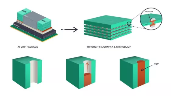
Innovative solutions in memory and processing architecture are needed – most notably, high-bandwidth memory (HBM) enabled by advanced packaging.
Traditional chip design limitations highlight the importance of advanced packaging
Historically, chip design advancements have followed Moore’s Law, which predicted that the number of transistors on a microchip would double approximately every two years, leading to improved performance. However, this trend is facing physical and technical limitations.
Conventional chip designs must be revamped to meet AI’s high-speed data transfer and low-latency demands. These limitations drive the semiconductor industry to explore advanced packaging solutions that can integrate multiple chips into a single package, enhancing performance and efficiency while extending Moore’s Law.
To read the full article, click here
Related Chiplet
- eFPGA Chiplet
- DPIQ Tx PICs
- IMDD Tx PICs
- Near-Packaged Optics (NPO) Chiplet Solution
- High Performance Droplet
Related News
- SCHMID Group Expands Advanced Packaging Portfolio to Power the AI Era
- Silicon Box Ships 100M Units, Proves Advanced Panel-Level Packaging Ready for AI, HPC era
- Applied Materials Introduces New Systems to Accelerate DRAM and Advanced Packaging for AI Chips
- KLA Unveils Comprehensive IC Substrate Portfolio for a New Era of Advanced Semiconductor Packaging
Latest News
- As AI Moves from Training to Inference, Optics Moves Closer to the Chip
- Arteris Announces Collaboration with IC-Link by imec to Accelerate Next-Gen AI and HPC Silicon
- Asahi Kasei Adds New Slitting Facility for SUNFORT™ to Meet Growing Demand for Advanced Semiconductor Packaging
- ACCM Introduces Celeritas SMC: A Production-Ready, Silicon-Matched Core for Advanced Packaging
- Socionext Addresses Datacenter Infrastructure Customer Demands for Advanced SoCs on TSMC A14 Technology