Adeia and UMC Expand Long-Term Collaboration in Hybrid Bonding Technologies
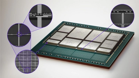
SAN JOSE, Calif., March 11, 2026 -- Adeia Inc. (Nasdaq: ADEA), the technology company known for developing foundational innovations that enable next-generation solutions for the semiconductor and media industries, today announced that it has expanded and renewed its intellectual property (IP) licensing relationship with United Microelectronics Corporation (UMC), a leading global semiconductor foundry. The new agreement provides UMC with continued access to Adeia’s semiconductor portfolio, including hybrid bonding technologies, and extends the companies’ collaboration into future generations of 3D integration and advanced packaging solutions.
 “The industry is seeing growing demand for chiplet architectures, driven by AI but also across diverse applications from networking to automotive. Leveraging our partnership with Adeia, UMC has unlocked significant value for customers through the successful 3D integration of RFSOI wafers for RF front-end modules,” said Steven Hsu, Vice President of Technology Development at UMC. “UMC is pleased to deepen this collaboration as we expand our advanced packaging services, providing customers with greater flexibility to integrate different types of wafers to meet the evolving needs of next-generation applications.”
Adeia’s portfolio of semiconductor IP includes industry-defining innovations in hybrid bonding, advanced packaging, and semiconductor processing technologies. These foundational technologies enable tighter interconnect pitch, improved power efficiency, greater bandwidth and increased reliability—critical enablers for next-generation logic, memory, AI accelerators, and high-performance computing devices.
“We are pleased to expand and extend our partnership with UMC, a respected leader in semiconductor manufacturing,” said Dr. Mark Kokes, chief revenue officer of Adeia. “Our innovations in hybrid bonding and advanced interconnect technologies are helping shape the future of semiconductors. This agreement reflects the strength of our IP portfolio and our commitment to supporting UMC as they continue to drive advancements in 3D integration and heterogeneous packaging.”
For more than 30 years, Adeia has pioneered structure, process and materials-level innovations that have become essential to advanced semiconductor products. The company’s IP is broadly licensed across the global semiconductor ecosystem and continues to support high-density, high-efficiency, and high-performance device architectures.
About Adeia Inc.
Adeia (Nasdaq: ADEA) is the technology company known for developing foundational innovations that enable next-generation solutions for the semiconductor and media industries. We invent and license technologies that shape the future of digital entertainment, electronics and high-performance computing. Adeia’s IP portfolio transforms technologies into experiences that are intelligent, immersive and personal. For more information, please visit www.adeia.com
Related Chiplet
- Integrated voltage regulator (IVR) chiplet
- High-performance connectivity chiplets
- eFPGA Chiplet
- DPIQ Tx PICs
- IMDD Tx PICs
Related News
- Adeia Demonstrates Hybrid Bonding Technology During Chiplet Summit 2024
- Adeia Presents Metrology Techniques for Improved Yield in Hybrid Bonding at IMAPS Device Packaging Conference 2024
- Adeia’s Pioneering Hybrid Bonding Technology Continues to Capture Attention
- Adeia at WLPS 2025: Advancing Hybrid Bonding Metrology
Latest News
- AI Data Centers Push Silicon Photonics Toward 300-mm Scale
- TYLsemi De-Risks Chiplets With New Business Model
- Cadence Introduces AuraStack AI Super Agent, the World’s First Agentic AI Platform for PCB and Advanced Packaging
- Saras Micro Devices Strengthens Senior Leadership Team to Scale Advanced Packaging Technology and Customer Growth
- TYLsemi Raises $43 Million to Launch First Full-Stack Chiplet Platform for Custom AI Silicon