When does it make sense to move from a monolithic ASIC to a chiplet-based design?

A journey into the benefits, trade-offs and technical implications of moving to chiplets
Monolithic integration and chiplet architectures in current ASIC design
Monolithic integration has been the dominant paradigm since the rise of VLSI-based ASICs in the 1970s–1980s. In a monolithic design, all functional blocks of integrated circuits such as logic, memory, analog interfaces, and specialized accelerators, are integrated onto a single piece of silicon. This model offers a compact, tightly coupled architecture with well-established design and verification flows.
However, the continued scaling of transistor dimensions and the growing complexity of modern systems are pushing the limits of this approach. As chip areas increase and advanced process nodes become more expensive and yield-sensitive, fabricating all functionality on a single die introduces significant cost, risk, and inflexibility.
In the last 5–10 years, chiplet-based architectures have begun to gain meaningful traction. Rather than integrating all components onto one large die, this approach partitions systems into multiple smaller dies –chiplets– each optimized for a specific function. The chiplets are manufactured independently and later assembled into a single package using advanced interconnect technologies.
While chiplets promise flexibility, cost savings, time to market, and scalability, they also introduce new complexities. This article explores when and why it makes sense to transition to a chiplet-based design, and under what circumstances monolithic ASICs remain the better choice.
Why chip designers are turning to chiplets
The main drivers for choosing chiplet-based designs are chip silicon die size and cost. In advanced designs, particularly those for AI, high-performance computing, and data center applications, the silicon area required for all functionality on a single die can approach or exceed the reticle size limit of modern lithography tools (i.e., the 26×33 mm area of the photomask used in 12-inch wafer lithography). Beyond this threshold, monolithic integration becomes infeasible; even before it, larger dies are more prone to defects, which reduces yield and increases cost. A single fault can compromise an entire chip, resulting in substantial cost losses.
Die size is tightly linked to what is arguably the most critical economic reason: the cost of silicon. Fabricating large monolithic dies at advanced nodes (e.g., 5nm or 3nm) is exponentially more expensive than at more mature nodes due to both process complexity and reduced yield. Advanced nodes require more intricate lithography, additional process steps, and higher-cost mask sets, all of which raise baseline manufacturing cost. When die size is large, these costs are further amplified by lower yield: the probability that a die contains one or more defects increases with area, making a significant fraction of dies non-functional and to be discarded. Chiplet-based designs avoid this by distributing functionality across smaller dies –which have a statistically higher chance of being defect-free– and only assembling known-good dies into the final package. In practice, chiplet yields can exceed 50%, while large monolithic designs of similar total area may drop below 30%.
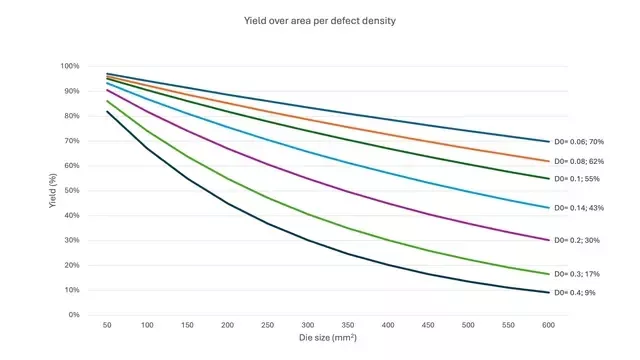
As total die area increases, chiplet-based designs consistently achieve higher yield than monolithic chips (D0 = defect density). Graph courtesy of IC-Link by imec.
Another important driver is heterogeneous integration. Many complex systems include functional blocks with vastly different requirements, for example, high-speed digital logic, low-power analog interfaces, embedded memory, and specialized accelerators. These blocks often perform best, or most cost-effectively, on different process nodes. In monolithic designs, all blocks must be implemented on the same substrate and process node, often leading to compromises in performance or cost. A chiplet architecture allows each subsystem to be implemented in the most suitable technology and later integrated at the package level. Proven IP blocks from older designs, such as analog front ends, can be retained as-is, while only the critical digital logic is updated to a newer node, thereby reducing development time and risk.
Chiplets also introduce modularity and reusability at the architectural level. Once a chiplet has been validated and qualified, it can be reused across multiple designs without repeating the full design and verification cycle. This approach supports faster iterations, for example when updating system functionality or targeting different performance or feature configurations. Moreover, it aligns with a growing industry vision to develop standardized chiplets that can be sourced off the shelf, enabling faster time-to-market, reduced development cost, and a competitive ecosystem of interoperable components.
Finally, chiplet architectures offer advantages in scalability: new functionality can be added by integrating an additional chiplet, without redesigning the entire system. If a design issue arises in a single block, only that chiplet needs to be reworked or requalified, reducing risk and accelerating development compared to full-chip reworks in monolithic flows.
When monolithic designs still make sense
Despite the growing interest in chiplet-based architectures, monolithic ASICs remain the preferred choice in many situations. The primary reason is architectural simplicity: integrating all functionality on a single die avoids the additional design, testing, and packaging complexities introduced by chiplet partitioning. Established verification flows, known failure modes, and mature tool support make monolithic development more straightforward.
Testing is also more straightforward. Monolithic designs benefit from established design-for-test (DfT) methodologies, supported by existing tools. Because all functions reside on a single die, there is no need to coordinate tests across dies or account for potential failure modes in interconnects. This makes system-level validation more streamlined and predictable than in chiplet-based designs.
Monolithic designs also offer tight integration between functional blocks, minimizing interconnect latency and maximizing bandwidth. For applications with strict timing constraints, such as communication between tightly coupled compute cores or between a processor and a shared memory block, even small delays can degrade performance. In these cases, the physical proximity of blocks on a single die remains a key advantage.
Moreover, chiplet-based approaches introduce system-level uncertainties that are still being addressed by the industry: packaging standards, DfT strategies, and long-term reliability under thermal and mechanical stress are areas of active development.
Therefore, for systems that do not push die area limits or require heterogeneous integration, the benefits of monolithic simplicity may outweigh the modularity and flexibility offered by chiplets.
What engineering challenges come with choosing chiplets?
While monolithic integration remains the more straightforward option in many contexts, the potential benefits of chiplets can warrant the additional complexity. If the decision is made to move to a chiplet-based architecture, however, it comes with a new set of engineering challenges.
A key consideration is partitioning strategy: which functional blocks can be isolated without compromising latency, bandwidth, or timing?
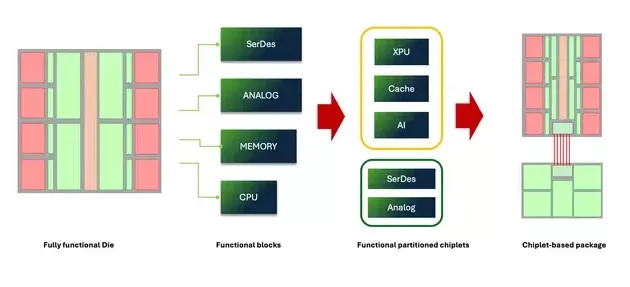
Functional blocks from a traditional SoC are partitioned into chiplets (e.g., CPU, memory, analog) and reassembled in a single package, enabling heterogeneous integration and improved yield. Diagram courtesy of IC-Link by imec
The first step is to assess technically feasibility of partitioning. Functional blocks that require tight timing or high bandwidth between them are often difficult to separate without introducing unacceptable latency. In contrast, blocks with limited interaction, such as analog versus digital logic or standalone accelerators, are generally better suited for chiplet partitioning. Another important factor is process node optimization. Analog circuitry, for example, typically performs well on mature nodes, while digital cores benefit from advanced scaling. Splitting these blocks across chiplets enables the use of advanced process technologies where they offer the most impact, without applying their associated cost across the entire design.
Partitioning, however, adds complexity to testing and verification. Each chiplet must be validated independently, and again as part of the assembled system including its inter-chiplet connections. Designers may need to insert test logic at both the die and package levels, and may require separate power delivery for individual dies, making power delivery more complex than in monolithic flows. Furthermore, die-to-die interconnects introduce new failure modes and verification challenges that are still being explored across the industry.
While support is improving, EDA flows for chiplet design, system-level test modeling standards, interconnect simulation, and thermal modeling are not yet as robust as those for monolithic design. Standards such as UCIe (Universal Chiplet Interconnect Express) aim to simplify multi-die integration but applying them in practice, especially in constrained domains like automotive, remains challenging. In these environments, strict requirements around mechanical reliability and packaging often conflict with standard interface assumptions. For example, current specifications allow for vertical via connections through the substrate, but such structures are not acceptable in high-reliability applications due to concerns around mechanical stress and long-term durability. Additionally, these standards not only address physical and protocol-level interoperability but are also evolving to support system-level requirements such as safety, security, and testability.
Thermal and physical constraints also influence how chiplets are placed within the package. Power density can be distributed more effectively across a chiplet system, which may simplify cooling in some designs. But this advantage depends on careful placement and routing: hotspots, long interconnect paths, or routing congestion can degrade system performance. At the same time, physical layout constraints, such as limited substrate routing resources, can restrict how chiplets are positioned and connected.
Applications where chiplets shine (and where they don’t)
So how do we decide between monolithic and chiplet-based integration? In the end, much depends on the specifics of the application: performance targets, system complexity, packaging constraints, cost sensitivity, and qualification requirements all influence the optimal architecture.
In domains such as data centers, high-performance computing and AI, chiplets have become increasingly more attractive. These systems often require large die areas to accommodate compute and memory subsystems, pushing against reticle limits and increasing the risk of yield loss. Chiplets allow compute and memory blocks to be split across multiple dies, each potentially built on a different node, and spread thermal load more effectively. Partitioning also enables the reuse of validated components across multiple system configurations, which supports scalable design roadmaps.
Automotive applications, particularly for advanced driver-assistance systems (ADAS) and autonomous compute platforms, are also moving toward chiplet integration;
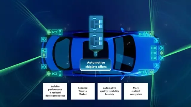
Chiplet integration in automotive systems can support scalability, faster development, and enhanced reliability. Visual content courtesy of imec.
These systems often require large, heterogeneous SoCs with strict reliability requirements. Chiplets can help by isolating critical functions across separate dies and allowing subsystems to be tested independently before final assembly. Today, adoption remains limited because standards like UCIe are still in early stages and not yet broadly validated for mechanical robustness, thermal stress, and long-term reliability. Once these packaging and qualification challenges are addressed, redundancy techniques, for example duplicated compute blocks to cross-check results, can be implemented into the chiplet domain.
In contrast, some use cases continue to favor monolithic integration, even at high complexity. For example, in financial trading systems, latency is the principal concern. Even microsecond-level delays introduced by inter-chiplet communication is problematic. In this domain, large monolithic dies remain the architecture of choice, despite the higher cost, because they provide consistent performance and minimize communication delays between tightly coupled functional blocks.
IoT and mobile devices also typically favor monolithic integration because they prioritize minimal size, low power consumption, and tightly integrated functionality. These requirements make the added complexity of chiplet packaging unjustified.
As packaging standards mature and system-level qualification processes evolve, chiplets may offer emerging advantages in new domains. In (aero)space applications, for instance, fault tolerance is typically achieved by using multiple redundant chips at the system level. By integrating redundancy within a chiplet-based package, it may be possible to reduce system complexity and improve efficiency while maintaining robustness.
Will chiplets become the new standard?
The transition from monolithic ASICs to chiplet-based architectures is not a binary shift, but a spectrum of trade-offs shaped by design constraints, application demands, and technological maturity. Chiplets offer compelling advantages when systems push against die size limits, require heterogeneous integration, or benefit from modularity and reuse. In such contexts, the ability to selectively use advanced nodes, manage thermal density, and iterate more flexibly can outweigh the additional complexity introduced by partitioning. Moreover, this architectural shift is supported by advances in packaging and substrate technology: improvements in interposer materials, bump pitch, and routing density now allow chiplets to be placed closer together, enabling higher bandwidth, lower energy per bit, and reduced parasitics.
At the same time, monolithic integration remains the preferred option when simplicity, latency, and tightly coupled functionality are paramount. Established design flows, mature tooling, and predictable performance continue to make monolithic ASICs an efficient solution, especially for small, low-power, or latency-critical applications.
Will chiplets become the default integration strategy in the next five to ten years? Unlikely. Chiplets represent a complementary architectural strategy, not a replacement for all design approaches. In the years ahead, monolithic and chiplet-based approaches will continue to coexist, each selected based on the specific requirements of the system being built.
Related Chiplet
- Integrated voltage regulator (IVR) chiplet
- High-performance connectivity chiplets
- eFPGA Chiplet
- DPIQ Tx PICs
- IMDD Tx PICs
Related Blogs
- How to Make Chiplets a Viable Market
- From Monolithic SoCs to Chiplets: A New Hardware Security Paradigm
- From Spec to Silicon: Successful Physical AI System Chiplet Bring-Up
- Topology and Data Movement in Multi-Die Design
Latest Blogs
- The Bottleneck Isn’t Compute. It’s Getting the Chip Built!
- How Intel Foundry Packaging Technologies Redefine AI and HPC Scalability Limits at ECTC 2026
- From complexity to simplicity: Scaling and future-proofing chiplets with AMBA®︎ CHI C2C property negotiation
- High-Speed Heterogeneous Integration with Multiphysics Analysis for TSMC SoW-X
- Chiplet Realization Beyond the Package: Why the Next AI Bottleneck Moves to the Interposer-to-PCB Boundary