CoWoS, wafer-scale and CoWoP: Why AI packaging bottleneck is moving

Advanced AI systems are forcing the semiconductor industry to rethink the boundary between silicon, package, board, power delivery, memory, cooling, and manufacturing. For several years, the dominant discussion has centered on advanced packaging capacity, high-bandwidth memory (HBM) integration, large interposers, organic substrate constraints, glass-core substrates, and scaling limits of 2.5D and 3D integration.
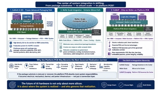 That discussion remains valid. But a deeper system question is emerging. What happens if the package substrate is no longer the center of the system-integration hierarchy? This question becomes especially important when comparing three architectural directions:
- CoWoS-style 2.5D integration
- Wafer-scale integration
- CoWoP/chip-on-wafer-on-platform-PCB concepts
Each approach is trying to solve the same industry problem: how to scale AI compute density, memory bandwidth, transient power delivery, thermal control, and multi-die integration beyond the physical limits of conventional packaging stacks. However, each architecture moves the bottleneck to a different place.
Chip-on-Wafer-on-Substrate (CoWoS) makes advanced packaging central to AI and high-performance compute (HPC) scaling. Next, wafer-scale integration pushes silicon integration to the extreme. Finally, Chip-on-Wafer-on-PCB (CoWoP) may create a new middle architecture where the platform PCB becomes part of the governed realization corridor.
To read the full article, click here
Related Chiplet
- Integrated voltage regulator (IVR) chiplet
- High-performance connectivity chiplets
- eFPGA Chiplet
- DPIQ Tx PICs
- IMDD Tx PICs
Related Blogs
- What is a Chiplet, and Why Should You Care?
- Introduction to Chiplets: Why the Industry is Moving Beyond Monolithic Designs
- AI Energy Gap and Chiplets: Why Data Movement Matters
- Addressing AI and Advanced Packaging Challenges with Synopsys 3DIO PHY
Latest Blogs
- When EMC Shielding Must Bend With the Package
- The Bottleneck Isn’t Compute. It’s Getting the Chip Built!
- How Intel Foundry Packaging Technologies Redefine AI and HPC Scalability Limits at ECTC 2026
- From complexity to simplicity: Scaling and future-proofing chiplets with AMBA®︎ CHI C2C property negotiation
- High-Speed Heterogeneous Integration with Multiphysics Analysis for TSMC SoW-X