InPsytech Highlights UCIe Innovation at COMPUTEX with UCIe Live Demo and Ultra-high speed ONFI 6400 Development
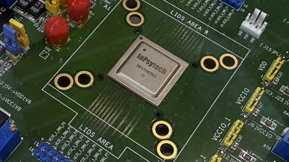
Hsinchu, Taiwan, June 4, 2026 — InPsytech, a leading provider of high-speed semiconductor IP solutions and a member of the Egis Group, is presenting a live demonstration of its Universal Chiplet Interconnect Express (UCIe) 3.0 solution, implemented on a 6nm process node in Computex 2026. The demo, currently running on-site, achieves data rates of up to 24Gbps per lane.
 The 6nm implementation interoperates with InPsy’s UCIe IP across multiple process nodes, including 3nm, 4nm, 5nm, and 12nm, demonstrating a comprehensive mixed-node integration solution. This capability supports the practical and scalable heterogeneous chiplet architectures combining compute dies, memory expansion dies, switch dies, and optical interconnect (EIC) dies from different technology nodes, enabling optimized partitioning of functionality across process technologies.
To further support system-level integration, InPsy enables protocol bridging across widely adopted on-chip interconnect standards, including AXI4, AXI-Stream, CXS, and CHI, leveraging the UCIe streaming protocol. These capabilities are designed to sustain high traffic throughput, low latency and deterministic performance. The architecture incorporates end-to-end flow control mechanisms to avoid congestion and optimize data movement across chiplets, facilitating a smooth transition from traditional monolithic SoC architectures to modular chiplet-based designs.
InPsy’s 6nm UCIe implementation also emphasizes energy efficiency, featuring a per-lane power gating mechanism that dynamically enables or disables individual lanes based on workload demand. Combined with optimized PHY architecture and low-power signaling, this approach significantly reduces active and idle power consumption, making it well-suited for energy-sensitive applications such as AI acceleration, hyperscale data centers, and high-performance computing.
InPsy is also highlighting the recent kickoff of its ONFI 6400 project, a next-generation NAND interface initiative targeting 6400MT/s signaling speeds to support future high-throughput storage systems. The project is on a 4nm process node and will serve as a platform for demonstrating high-speed signaling integrity, advanced equalization techniques, and controller interoperability for next-generation NAND ecosystems.
“Chiplet architecture is rapidly becoming a cornerstone of next-generation semiconductor innovation. Our UCIe solution demonstrates not only strong performance and flexibility across process nodes, but also a system-level approach that enables our customers to build more scalable and power-efficient designs,” said Howard Ro, Chief Executive Officer of InPsy. “Together with the advancement of our ONFI 6400 project, we are reinforcing our commitment to driving future high-performance computing and data infrastructure.”
About InPsytech
InPsytech is a Taiwan-based silicon IP company specializing in high-performance interface, memory, and interconnect IP solutions. The company is dedicated to empowering SoC designers through robust, scalable IP optimized for applications in AI, data centers, mobile, and edge computing. InPsy partners with foundries worldwide and design ecosystems to deliver IP solutions that accelerate time-to-market and enable next-generation semiconductor innovations. For more information, please visit https://www.inpsy.com
Related Chiplet
- Integrated voltage regulator (IVR) chiplet
- High-performance connectivity chiplets
- eFPGA Chiplet
- DPIQ Tx PICs
- IMDD Tx PICs
Related News
- Qualitas Semiconductor Successfully Demonstrates Live UCIe PHY IP at AI Infra Summit 2025
- InPsytech Announces Finalization of UCIe IP Design, Driving Breakthroughs in High-Speed Transmission Technology
- InPsytech Tapes Out F2F SoIC Design Compliant with UCIE 2.0 Standard Enabling High-Speed Interconnects for 3D Heterogeneous Integration
- InPsytech showcases 3nm UCIe 3.0 technology at OCP 2025, Accelerating Innovation in Chiplet Ecosystem
Latest News
- AI Data Centers Push Silicon Photonics Toward 300-mm Scale
- TYLsemi De-Risks Chiplets With New Business Model
- Cadence Introduces AuraStack AI Super Agent, the World’s First Agentic AI Platform for PCB and Advanced Packaging
- Saras Micro Devices Strengthens Senior Leadership Team to Scale Advanced Packaging Technology and Customer Growth
- TYLsemi Raises $43 Million to Launch First Full-Stack Chiplet Platform for Custom AI Silicon