Are ghiplets the next evolution stage in GPU designs?
By Majeed Ahmad, EDN (April 1, 2024)
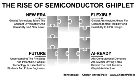
When GPUs are implemented in a chiplet arrangement, can they be called ghiplets? Semiconductor industry professional Chetan Arvind Patil thinks so. In his blog “The Rise of Semiconductor Ghiplet”, Patil outlines the benefits of GPUs in chiplet architectures compared to monolithic GPU designs currently struggling with lower yield rates for large and complex GPU devices.
In other words, all the rendering is handled by chiplets instead of a big-compute GPU. Take the case of AMD’s Radeon RX 7000 series, one of the first chiplet-based GPUs, which incorporates a large graphics die and several memory dies. The Silicon Valley-based semiconductor firm is now considering using even more chiplets in a GPU design.
To read the full article, click here
Related Chiplet
- Optical Chiplet
- Reverse Gearbox Chiplet
- FlexGen Multi-Die Smart Network-on-Chip (NoC) IP
- Ncore Multi-Die Interconnect IP
- Integrated voltage regulator (IVR) chiplet
Related News
- New AMD Patent Describes Potential Chiplet-Based GPU Design
- How to Build a Better “Blackwell” GPU Than Nvidia Did
- Safety architecture boosts automotive GPU for chiplets
- Intel patents chiplet GPU design
Latest News
- Silicon Austria Labs Adopts PulseForge Photonic Debonding Technology to Accelerate Advanced Packaging and Heterogeneous Integration Research
- Powerlattice Demonstrates Industry’s First Monolithic IVR Chiplet to Break the AI Power Wall
- Von Aredenne Addresses Semiconductor Panel-Level Packaging Market with New HiPIMS Deposition Solution
- PFN and Tenstorrent Selected for NEDO Project on “xPU Design and Development Incorporating Photonics Electronics Integration Technology”
- Tenstorrent Releases Open Source Beta of the Open Chiplet Atlas® (OCA) Harness