Ready to go just in time for the EU visit: Fraunhofer IMS Unveils New Photonics Laboratory in Duisburg
June 16, 2026 -- Light travels fast, and in the new photonics laboratory at the Fraunhofer Institute for Microelectronic Circuits and Systems IMS, it is now doing the work on the chip. The institute has launched a photonics lab that enables it to develop, manufacture, and characterize photonic chiplets entirely on-site: from the initial idea to the characterized component, as a full-fledged contribution to the European APECS pilot line. Several key pieces of equipment for the new lab were acquired with funding from the APECS pilot line. A high-ranking guest from Brussels, Dr. Eric Fribourg-Blanc, Senior Programme Officer at the European Union’s Chips Joint Undertaking, visited the institute and got a firsthand look at the current state of affairs.
Why Photonic Chiplets Are Important for All of Us
The name sounds cumbersome, but the principle behind photonic chiplets has long been part of everyday life. Fiber-optic cables that carry the internet operate on the same basic principle: instead of electrical signals, these components transmit light, enabling significantly higher speeds, better energy efficiency, and greater bandwidths than traditional electronics. In highly integrated systems of the future—such as those for data communication, medical sensors, or AI infrastructure—such photonic components will play a key role.
Fraunhofer IMS develops and manufactures these chiplets in its own cleanroom on 200-mm wafers under industry-standard conditions. The photonic integrated circuits (PICs) are implemented on CMOS readout circuits. In doing so, the institute directly links its core expertise in microelectronics with state-of-the-art photonics. This combination makes Fraunhofer IMS a sought-after partner within the European chiplet landscape.
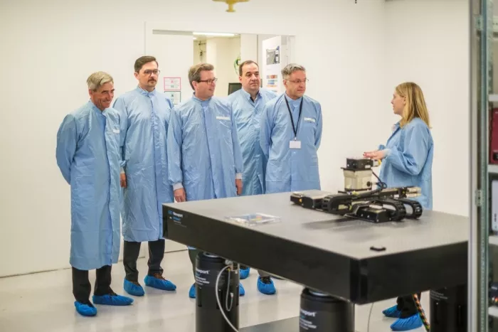
Tour of the new photonics laboratory
The new lab: 50 square meters that make all the difference
With the new photonics lab, Fraunhofer IMS is now introducing a complete characterization infrastructure into the European pilot line, thereby strengthening the common technological foundation of all APECS partners. Two optical measurement stations have been set up in a space of just under 50 square meters, enabling characterization at both the chip and wafer levels.
The first measurement setup is designed for the semi-automatic characterization of photonic circuits with grating couplers. A nanopositioning system with six degrees of freedom and an integrated rotary stage positions optical fibers and fiber arrays with microscopic precision at the chip’s light-coupling points, enabling precise optical coupling with photonic integrated circuits on wafers up to twelve inches in diameter. A second setup, also equipped with a nanopositioning system with six degrees of freedom, allows for the characterization of chips with side couplers.
Light sources available include a supercontinuum laser with a tunable wavelength range from 350 to 2400 nanometers and a narrow-band precision laser for the telecommunications sector centered at 1550 nanometers. The supercontinuum laser, together with tunable filters, enables comprehensive characterization of photonic wafers and chips from the UV to the near-infrared range. A spectrometer complements the measurement infrastructure for the evaluation of optical signals.
“With the new photonics laboratory, we can now develop and characterize our photonic chiplets entirely on-site, from the initial idea to the tested component. This gives the entire APECS network exactly the speed of execution that a European pilot line project of this magnitude requires,” says Prof. Dr. Anna Lena Schall-Giesecke, Head of Technology.
European technological sovereignty: more than just a buzzword
The laboratory setup is not an end in itself. As one of 15 institutes, Fraunhofer IMS is part of the Research Factory Microelectronics Germany (FMD) and a key contributor to APECS, the pilot line for “Advanced Packaging and Heterogeneous Integration for Electronic Components and Systems.” APECS is a key component of the EU Chips Act, designed to drive chiplet innovations and increase research and manufacturing capacities for semiconductors in Europe. The goal is to establish a comprehensive European pilot line to enhance Europe’s technological resilience, secure supply and value chains, and drive innovation in key industries.
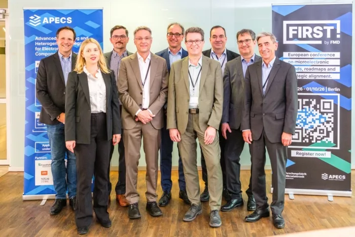
Visit by delegates from Chips JU and APECS
Dr. Fribourg-Blanc’s visit made it clear that Fraunhofer IMS plays no minor role in this effort. Following a welcome by Institute Director Prof. Dr. Anton Grabmaier and presentations by Prof. Dr. Anna Lena Schall-Giesecke, Dr. Alexander Litke, and Holger Kappert on cooperation activities, specific pilot line contributions, and planned procurement measures, the group headed straight to the lab, where Europe’s chip future is literally being measured.
Particular attention was paid to three areas of expertise that the institute brings to APECS: the development and fabrication of highly integrated photonic chiplets, a powerful design infrastructure for external users featuring customized design flows, process design kits, and simulation models, as well as the institute’s newly expanded characterization capabilities. Together, these building blocks are intended to provide companies of all sizes—from global corporations to technology startups—with low-threshold access to photonic chiplet technology.
A jointly developed multi-material sensor demonstrator illustrates how this works in practice; in this demonstrator, photonic chiplets from Fraunhofer IMS are integrated with technologies from other APECS partners on a common interposer to form a functional heterogeneous system.
“For Fraunhofer IMS, APECS is far more than just a research project. It is a concrete contribution to Europe’s technological independence. Photonic chiplets are a key technology for the systems of tomorrow, and we are delighted to be developing this building block together with our European partners,” emphasizes Dr. Alexander Litke, project manager for APECS activities at Fraunhofer IMS.
Related Chiplet
- eFPGA Chiplet
- DPIQ Tx PICs
- IMDD Tx PICs
- Near-Packaged Optics (NPO) Chiplet Solution
- High Performance Droplet
Related News
- Fraunhofer IMS Takes a Key Role in Establishing the APECS Pilot Line
- Fraunhofer IIS/EAS Selects Achronix Embedded FPGAs (eFPGAs) to Build Heterogeneous Chiplet Demonstrator
- U.S. Navy Funds Mercury to Develop Photonics Chiplet Manufacturing Capability for Defense Applications
- Innovation in the semiconductor market: chiplets pave the way to the future
Latest News
- TYLsemi Raises $43 Million to Launch First Full-Stack Chiplet Platform for Custom AI Silicon
- SILITH and UMC Achieve Mass Production Milestone for Silicon Photonics
- As AI Moves from Training to Inference, Optics Moves Closer to the Chip
- Arteris Announces Collaboration with IC-Link by imec to Accelerate Next-Gen AI and HPC Silicon
- Asahi Kasei Adds New Slitting Facility for SUNFORT™ to Meet Growing Demand for Advanced Semiconductor Packaging