Chiplets, Ecosystems, and Europe’s Post-Fab Semiconductor Strategy
As AI drives semiconductor complexity beyond monolithic design, Europe sees its future competitiveness in chiplets, interoperability, and heterogeneous integration.
By Pat Brans, EE Times | May 28, 2026
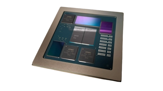
For years, Europe’s semiconductor ambitions were measured in fabs, process nodes, and manufacturing sovereignty. The European Chips Act elevated semiconductors to the level of strategic industrial policy, triggering a wave of subsidies and investment proposals aimed at rebuilding manufacturing capacity across the continent.
Yet despite those efforts, Europe’s position in the global semiconductor industry continues to weaken. Few executives have watched Europe’s semiconductor industry evolve as closely as Maria Marced, who now helps shape discussions around Chips Act 2.0. According to Marced, Europe’s global semiconductor market share could fall to around 6% this year.
To read the full article, click here
Related Chiplet
- Optical Chiplet
- Reverse Gearbox Chiplet
- FlexGen Multi-Die Smart Network-on-Chip (NoC) IP
- Ncore Multi-Die Interconnect IP
- Integrated voltage regulator (IVR) chiplet
Related News
- Automotive Meets Chiplets: Robert Bielby’s Perspective on the Impact of Level 3 ADAS on Emerging Semiconductor Tech
- Chiplets: Revolutionizing Semiconductor Design and Manufacturing
- The Role of Chiplets in Redefining Semiconductor Design
- DreamBig Semiconductor Announces Partnership with Samsung Foundry to Launch Chiplets for World Leading MARS Chiplet Platform on 4nm FinFET Process Technology Featuring 3D HBM Integration to Solve Scale-up and Scale-out Limitations of AI for the Masses
Latest News
- Amkor Technology and NVIDIA Advance Strategic Partnership for AI Infrastructure
- Siemens expands agentic AI collaboration to tackle 3D IC power and thermal challenges with NVIDIA
- Photon Bridge Raises €10M to Tackle AI’s Emerging Laser Bottleneck
- Abacus Semiconductor and Aalto University Announce Research Cooperation on High-Speed Chiplet Interconnects
- UK Launches Semiconductor Catapult to Strengthen Sovereign Capabilities in AI Hardware and Defence