Arm’s Chiplet System Architecture eyes ecosystem sweet spot
By Majeed Ahmad, EDN (January 27, 2025)
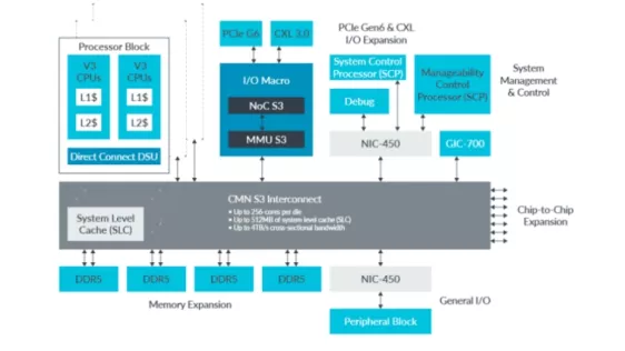
Arm has announced the availability of the first public specification drafted around its Chiplet System Architecture (CSA), a set of system partitioning and chiplet connectivity standards harnessed in a design ecosystem supported by over 60 companies. The companies that are part of the CSA initiative include ADTechnology, Alphawave Semi, AMI, Cadence, Jaguar Micro, Kalray, Rebellions, Siemens, and Synopsys.
CSA aims to offer industry-wide standards and frameworks by facilitating the reuse of specialized chiplets, and thus address the fragmentation caused by compatibility issues in chiplet design. It provides a shared understanding of defining and connecting chiplets while developing composable system-on-chips (SoCs).
A couple of recent announcements show how semiconductor firms are employing CSA to build chiplets as part of Arm Total Design, a platform for deploying chiplet-based compute subsystems. Arm Total Design facilitates custom silicon solutions powered by Arm Neoverse Compute Subsystems (CSS), which includes processor cores, IPs, software, and design tools.
To read the full article, click here
Related Chiplet
- Optical Chiplet
- Reverse Gearbox Chiplet
- FlexGen Multi-Die Smart Network-on-Chip (NoC) IP
- Ncore Multi-Die Interconnect IP
- Integrated voltage regulator (IVR) chiplet
Related News
- Arm Chiplet System Architecture Makes New Strides in Accelerating the Evolution of Silicon
- Eliyan joins Arm Total Design ecosystem to accelerate chiplet economy
- Cadence Collaborates with Arm to Jumpstart the Automotive Chiplet Ecosystem
- Cadence Launches Partner Ecosystem to Accelerate Chiplet Time to Market
Latest News
- Amkor Technology and NVIDIA Advance Strategic Partnership for AI Infrastructure
- Siemens expands agentic AI collaboration to tackle 3D IC power and thermal challenges with NVIDIA
- Photon Bridge Raises €10M to Tackle AI’s Emerging Laser Bottleneck
- Abacus Semiconductor and Aalto University Announce Research Cooperation on High-Speed Chiplet Interconnects
- UK Launches Semiconductor Catapult to Strengthen Sovereign Capabilities in AI Hardware and Defence