AI Competition Turns into a Supply Chain Arms Race, Tightening Advanced Packaging and 3nm Capacity
April 30, 2026 -- TrendForce’s latest foundry industry findings point out that AI demand has surged rapidly since 2023, leading to capacity bottlenecks in 3 nm–2 nm wafers and 2.5D/3D advanced packaging. The shortage of CoWoS has persisted, extending upstream to production equipment and downstream to substrates, packaging materials, and other critical components.
On the front-end, 3nm advanced process capacity—currently dominated by TSMC—has become even more constrained, turning into a scarce resource fiercely contested by global tech giants.
TrendForce notes that the resource competition triggered by AI has spread across the entire semiconductor supply chain. Industry leader NVIDIA, leveraging its experience and strong supply chain control, was among the first to identify tightening capacity and preemptively secured large volumes of 4/3 nm wafer capacity, CoWoS packaging, as well as key materials such as T-glass, substrates, PCBs, HBM, and SSDs. While other tech giants like Google also have strong demand, delays in securing critical components have led to material shortages, constraining product growth.
The consumption of wafer and packaging resources per chip is increasing exponentially as the demand for AI compute drives larger chip sizes. Despite TSMC’s ongoing capacity expansion, CoWoS has remained in short supply since 2023, prompting customers to seek alternative capacity sources.
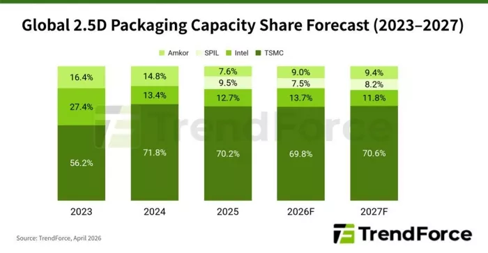
OSAT providers such as SPIL and Amkor have benefited from this spillover demand, and alternative technologies like EMIB and FOEB are also gaining traction, with Intel leveraging its U.S.-based manufacturing advantage.
TrendForce expects that the severe shortage in global 2.5D packaging capacity will begin to ease slightly by 2027, aided by order spillover and TSMC’s plan to expand CoWoS capacity by over 60% by 2027.
On the front-end process side, AI compute chips are rapidly transitioning from 4 nm to 3 nm between late 2025 and 2026. At the same time, high-end smartphone and PC processors have yet to migrate en masse to the next-generation 2 nm node, resulting in a short-term concentration of high-performance demand on 3 nm.
From a supply perspective, Samsung and Intel remain behind TSMC in 3 nm foundry progress. Combined with the fact that most chip designs are finalized one to three years in advance, this has led to a temporary single-supplier dynamic dominated by TSMC. The company is accelerating the construction of new 3 nm fabs to alleviate the imbalance. As additional capacity comes online, global 3 nm capacity is expected to surpass 5/4 nm by the end of 2026 and become the second-largest process node after 28 nm by 2027.
Related Chiplet
- Integrated voltage regulator (IVR) chiplet
- High-performance connectivity chiplets
- eFPGA Chiplet
- DPIQ Tx PICs
- IMDD Tx PICs
Related News
- Advanced Packaging Driving New Collaboration Across Supply Chain
- SCHMID Group Expands Advanced Packaging Portfolio to Power the AI Era
- Silicon Box Ships 100M Units, Proves Advanced Panel-Level Packaging Ready for AI, HPC era
- YES Selected to Deliver Full Portfolio of Advanced Packaging Tools for Glass Panel AI and HPC Applications by a Leading AI Infrastructure Supplier
Latest News
- Amkor Technology Announces Strategic Partnership with NVIDIA to Expand Advanced Packaging and Test for Next-Generation AI Infrastructure
- Synopsys Enables AMD Instinct™ MI455X GPU Design with Comprehensive Multi-Die Solution
- AI Data Centers Push Silicon Photonics Toward 300-mm Scale
- TYLsemi De-Risks Chiplets With New Business Model
- Cadence Introduces AuraStack AI Super Agent, the World’s First Agentic AI Platform for PCB and Advanced Packaging