AI and Chiplets Prominent at TSMC OIP 2025
By Majeed Ahmad, EETimes | September 26, 2025
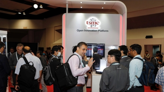
The design tool offerings of the top three EDA houses showcased at TSMC’s annual U.S. event once more affirm the two defining trends in the current semiconductor landscape: artificial intelligence (AI) and chiplets. TSMC’s Open Innovation Platform (OIP) Ecosystem Forum brings together partners to demonstrate their design advancements of TSMC’s latest process nodes and packaging technologies.
The EDA trio’s announcements at the event encompass new AI flows and multi-die innovations relating to 3D IC, advanced packaging, and chiplets. The advancements in AI and chiplet realms are intertwined, paving the way for high-performance AI and HPC chips that serve compute-intensive workloads.
To read the full article, click here
Related Chiplet
- Integrated voltage regulator (IVR) chiplet
- High-performance connectivity chiplets
- eFPGA Chiplet
- DPIQ Tx PICs
- IMDD Tx PICs
Related News
- Alphawave Semi and Arm to Present on Chiplets for Architecting Next-Generation Terabit AI Networks at the TSMC OIP Ecosystem Forum North America
- Lorentz Solution Jointly Presents with NVIDIA on Large-Scale 3D Terahertz EM Simulation for Real IC/3DIC Silicon Case Studies in Photonic Switches at 2025 TSMC OIP
- Teradyne Awarded 2025 TSMC Open Innovation Platform® (OIP) Partner of the Year for TSMC 3DFabric® Testing
- TSMC plans automotive chiplet process for 2025
Latest News
- Amkor Technology Announces Strategic Partnership with NVIDIA to Expand Advanced Packaging and Test for Next-Generation AI Infrastructure
- Synopsys Enables AMD Instinct™ MI455X GPU Design with Comprehensive Multi-Die Solution
- AI Data Centers Push Silicon Photonics Toward 300-mm Scale
- TYLsemi De-Risks Chiplets With New Business Model
- Cadence Introduces AuraStack AI Super Agent, the World’s First Agentic AI Platform for PCB and Advanced Packaging