The Unfinished Revolution
Advanced Packaging and Heterogeneous Integration
Amazing breakthroughs lie ahead. It won’t be easy -- but it will be awesome.
How it started
I remember when wafer-level stacking was brand new. It wasn’t “advanced packaging” back then. Even the term “3DIC” was brand new. The idea was audacious and stunning and we loved it.
We seized on multi-level memory as the ideal application for wafer stacking. We foresaw huge storage in a tiny footprint with terrific yield, better bandwidth, shorter latency, improved error detection – wow! Our process guys were closing in on robust copper thermocompression. Our design guys were inventing clever mechanisms for multilevel addressing and super-efficient 3D remapping. We were on fire.
Process separation
The extraordinary opportunity we saw in 3D memory was that each layer could be built independently. We could separate the high-performance elements from the memory cells, move them onto different layers, and build each layer in its optimal process. Ultra-low leakage layers for memory cells and slick high-speed layers for everything else: the best of both worlds in one device! We called it “process separation” because the layers were built in separate processes. We didn’t call it “heterogeneous integration” back then – but that’s what it was.
Mixed nodes
Another facet of the stacked solution: optimizing the technology node for each layer. Tiny leading-edge nodes give the best density; larger nodes are better for analog devices and high voltage operation. More than a decade ago our team used hybrid bonding to combine layers built at 40nm (high density DRAM cells), 65nm (high voltage I/O), and 45nm (good analog performance for sense amps, voltage regulators, and PLLs). Combining different processes and different nodes created what was, at the time, a revolutionary device.
Where are we today?
Fast-forward to now. 3DICs are everywhere. Even bigger than 3D is interposer technology – “2.5D integration” – which has mushroomed in ways we never saw coming. Chiplets are touted as the Next Big Thing. Integration of different processes and different nodes is commonplace.
And yet, some of the golden promises of heterogeneous integration are still on the table.
Specifically, today’s solutions do not take full advantage of mixed materials or mixed sources.
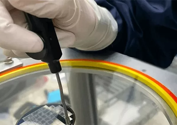
Selecting thin-film lithium niobate (TFLN) dies for 3D integration onto a silicon host wafer
– NHanced Semiconductors
“Incompatible” materials
There are “exotic” materials that radically outperform silicon in niche applications. Unfortunately, they fall short in many ways – fragility, extreme cost, odd wafer sizes, etc. Processing these materials requires totally different equipment and chemicals. On top of that, they pose a contamination risk in the manufacturing line. These materials are explicitly unwelcome in standard silicon foundries.
The dream is to incorporate specialized materials only where they are needed and build the rest in good old silicon. This is easier said than done. Bonding dissimilar materials takes “complicated” to an entirely new level. Beyond that looms a huge thermal issue: if the coefficients of thermal expansion don’t match, the bonded assembly is liable to warp, delaminate, or shatter altogether.
NHanced comes to this issue with a distinct advantage. Our Morrisville process team has a long and successful history with nonstandard materials. Working in the same fab where DBI® hybrid bonding was invented, they have developed artful engineering methods that achieve reliable outcomes.
Today, NHanced is the only commercial provider of mixed-material hybrid bonding.
The set of materials currently available for heterogeneous integration is limited; our team continually experiments and innovates with the goal of expanding that set.
Multi-sourcing
For all the talk of chiplets, there’s currently no easy way to assemble components from multiple vendors. Today’s chiplets are “siloed” – built and used within a single company. Someday, robust standards will create a thriving shared chiplet ecology. For now, it’s a logistical labyrinth. Manufacturers are in fierce competition with one another, each leveraging closely guarded industrial secrets. They can’t be expected to expose proprietary information to a random third party for assembly purposes.
Here again NHanced has an edge, thanks to our “Foundry 2.0” manufacturing model. We don’t compete with the “Foundry 1.0” manufacturers. In fact, we have existing relationships with almost all of them, having already collaborated on successful projects.
We are the “Switzerland” of foundries.
We can set up coordinated non-disclosure agreements for projects that would be otherwise unworkable. We’ve done hundreds of these already. Each is a new adventure with its own challenges, but we have a repeatable business flow.
What’s next?
Predictions are always risky. Nonetheless, here are a few sure bets:
- Leading-edge technology nodes will get even smaller.
- Leading-edge fabs will get even bigger.
- Advanced Packaging – 3D and 2.5D – will expand to serve broader markets.
- More materials will become commercially viable for stacking.
- Chiplets will start to support inter-company designs.
And my own personal prediction:
NHanced will maintain its lead, breaking new ground through technical innovation.
Related Chiplet
- Interconnect Chiplet
- 12nm EURYTION RFK1 - UCIe SP based Ka-Ku Band Chiplet Transceiver
- Bridglets
- Automotive AI Accelerator
- Direct Chiplet Interface
Related Blogs
- The Chiplet Revolution
- UCIe and Automotive Electronics: Pioneering the Chiplet Revolution
- Silicon Creations is Enabling the Chiplet Revolution
- The Chiplet Revolution
Latest Blogs
- 3D-IC Test and Reliability: KGD Strategies, Access Architecture, & Failure Mode
- 3D-IC in AI, HPC, and 5G: Bandwidth, Latency, and Energy per Bit Advantages
- Bosch and the chiplet revolution: Enabling software-defined mobility
- Addressing the Biggest Bottleneck in the AI Semiconductor Ecosystem
- Thermal Management in 3D-IC: Modeling Hotspots, Materials, & Cooling Strategies