3D ICs, Chiplets & HBM: How Packaging Is Driving the Semiconductor Roadmap

In the evolving world of semiconductors, performance gains are no longer driven solely by shrinking transistor nodes. As traditional Moore’s Law scaling starts to plateau, advanced packaging technologies like 3D Integrated Circuits (3D ICs), chiplets, and High Bandwidth Memory (HBM) are becoming central to enhancing compute performance, power efficiency, and form factor. These innovations are not just incremental improvements; they are redefining how chips are architected, manufactured, and deployed across industries.
The Limitations of Traditional Scaling
For decades, the semiconductor industry relied heavily on 2D scaling to improve performance. Smaller transistors meant faster speeds and lower power consumption. However, moving to nodes below 5nm is proving to be increasingly expensive and technically complex. Lithography limitations, interconnect bottlenecks, and thermal issues have forced top semiconductor company leaders to rethink their design and integration strategies.
This is where advanced packaging steps in, not as a support function, but as a central pillar of semiconductor innovation.
What Are 3D ICs?
3D Integrated Circuits (3D ICs) stack multiple layers of silicon vertically, enabling dense integration of different functions (e.g., logic, memory, I/O) into a compact footprint. This vertical stacking reduces signal distances, boosts performance, and significantly lowers power consumption. It also allows for heterogeneous integration, bringing together different process nodes and IPs that are otherwise hard to integrate in monolithic SoCs.
Benefits of 3D ICs:
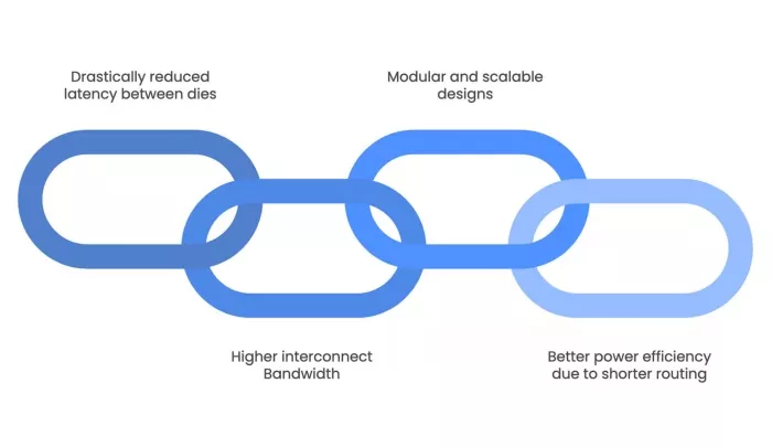
3D ICs are particularly valuable in domains like AI accelerators, high-performance computing (HPC), and networking areas where bandwidth and power efficiency are paramount.
Chiplets: The LEGO Blocks of Modern Chips
In the chiplet model, a large SoC is disaggregated into smaller functional units (chiplets), which are then assembled on an interposer or substrate. Each chiplet can be designed, fabricated, and validated separately, which helps reduce development time and cost. Moreover, companies can reuse proven IP chiplets across multiple designs.
AMD’s Ryzen and EPYC processors are well-known examples where multiple CPU chiplets are stitched together using Infinity Fabric to create powerful, scalable products.
Key Advantages of Chiplets:
- Flexibility in combining different technologies
- Yield improvements due to smaller die sizes
- Faster time-to-market
- Cost-effective customization
The chiplet approach aligns well with the increasing demand for customization in markets like edge AI, automotive, and enterprise infrastructure.
High Bandwidth Memory (HBM): Fueling Data-Hungry Workloads
Memory bandwidth has long been a bottleneck in high-performance computing. Enter High Bandwidth Memory (HBM), a vertically stacked memory architecture integrated close to the processor using 2.5D or 3D packaging techniques. By placing DRAM stacks on or near the logic die, HBM delivers significantly higher data transfer rates compared to traditional DDR or GDDR memory.
HBM2 and HBM3 are now common in GPUs, AI accelerators, and FPGAs that require massive bandwidth and low latency. With bandwidths exceeding 1 TB/s in some designs, HBM is unlocking new capabilities in scientific simulations, LLM training, and real-time analytics.
The Symbiosis of 3D ICs, Chiplets, and HBM
These three packaging technologies are not standalone trends; they work synergistically. For example, a next-generation AI accelerator may use:
- A 3D IC design for tight integration between compute cores and control logic
- Chiplets to incorporate customizable blocks such as security modules or signal processors
- HBM for ultra-high memory bandwidth to feed data-hungry compute engines
The convergence of these technologies allows a semiconductor design company to innovate faster while overcoming traditional node-scaling limitations.
Impact on Semiconductor Engineering & Design
The rise of advanced packaging has redefined the responsibilities and skill sets in semiconductor engineering. It’s no longer enough to master RTL design or circuit layout; today’s engineers must also understand packaging thermals, mechanical stress, die-to-die communication, and system-level co-design.
From thermal simulation tools to interconnect modeling, packaging now requires cross-functional collaboration across materials science, physics, software, and electrical engineering.
Furthermore, top semiconductor company R&D teams are heavily investing in new materials and die bonding techniques, such as hybrid bonding and through-silicon vias (TSVs), to enhance 3D integration and chiplet connectivity.
Real-World Use Cases Driving Packaging Innovation
1. AI and Machine Learning
AI workloads are notoriously memory-bound. Nvidia’s H100 uses HBM3 with 3D packaging to keep GPUs constantly fed with data, reducing idle time and improving inference throughput.
2. Automotive
ADAS (Advanced Driver-Assistance Systems) and autonomous driving platforms benefit from chiplets and 3D ICs by integrating sensor data processors, safety-critical compute blocks, and memory in a single module with low power and high reliability.
3. Data Centers
Hyperscalers are pushing for co-packaged optics (CPO) using chiplet and 2.5D integration to increase I/O density and reduce power consumption for data movement.
Why Tessolve Is a Key Enabler in Advanced Packaging
As an industry leader with end-to-end silicon and system expertise, Tessolve plays a pivotal role in advancing 3D ICs, chiplet integration, and HBM adoption. Tessolve offers comprehensive semiconductor engineering solutions, from IC design and high-speed board development to signal integrity, thermal analysis, and system validation. Our packaging support spans:
- Advanced substrate and interposer design
- Thermal and mechanical modeling
- Post-silicon validation and bring-up
- DFT and test program development
Tessolve’s ability to bridge the gap between silicon, packaging, and systems positions us as a go-to partner for any semiconductor design company looking to adopt cutting-edge integration techniques. With decades of experience and a global engineering workforce, Tessolve continues to accelerate time-to-market and de-risk development cycles for customers worldwide.
Conclusion: Packaging Is the New Silicon
The semiconductor roadmap is no longer driven solely by transistor scaling. Instead, 3D ICs, chiplets, and HBM have emerged as the foundational elements of innovation, offering modularity, scalability, and performance that traditional methods can’t match. These technologies are not just packaging; they are strategic enablers of product differentiation and leadership.
As the industry marches toward more heterogeneous, power-efficient, and high-performance systems, the importance of advanced packaging will only grow. For companies that aim to lead in AI, 5G, automotive, and high-performance computing, embracing these technologies is not optional; it’s imperative.
For startups and established giants alike, partnering with Tessolve, we offer the full spectrum of semiconductor engineering services from chip to system, is key to navigating this complex but rewarding landscape.
In this new era, packaging isn’t the final step; it’s the game-changer shaping the future of every top semiconductor company.
Related Chiplet
- DPIQ Tx PICs
- IMDD Tx PICs
- Near-Packaged Optics (NPO) Chiplet Solution
- High Performance Droplet
- Interconnect Chiplet
Related Blogs
- Designing the Future: How 3DIC Compiler Is Powering Breakthroughs Across the MultiDie Design Landscape
- What are Chiplets and how they Assemble Into the Most Advanced SoCs
- Driving the Development and Deployment of Chiplets in the Automotive Industry
- The Age of Chiplets is Upon Us
Latest Blogs
- Wafer-Scale vs. Chiplets: The new war?
- Chiplets 101: An Arteris Guide to Multi-Die Architecture
- 2.5D + 3D = “3.5D”!
- Addressing AI and Advanced Packaging Challenges with Synopsys 3DIO PHY
- Ultra-high repeatability and ultra-low insertion loss wafer and die-level visible-range E-PIC device characterization using an MPI Corp. probe system, enabled by process optimization from Quantum Transistors