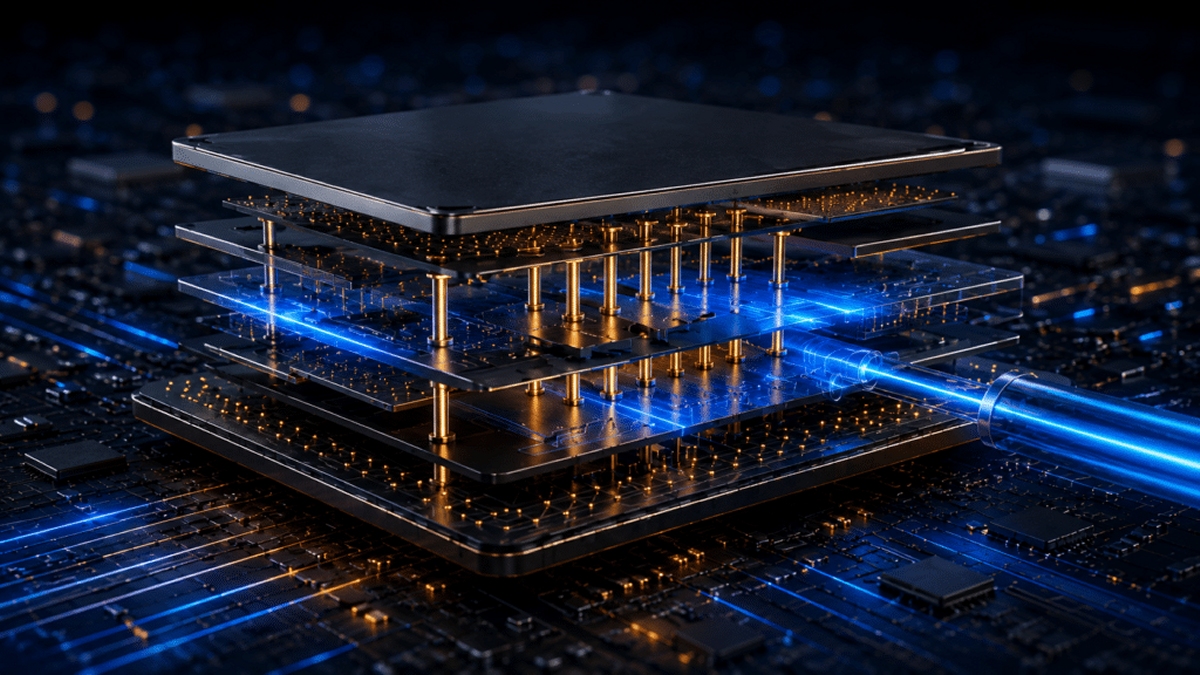
Atomica - Chiplet Ecosystem
Atomica is a U.S.-based microfabrication foundry offering advanced platforms for AI infrastructure, photonics, sensors, MEMS, and biotechnology microdevices.
We deliver rapid prototyping and scalable production to customers developing AI optical connectivity, AI optical source integration, AI photonic packaging, AI thermal microstructures, physical AI sensors, MEMS optical control systems, and biotechnology microdevices across optical communications, healthcare, aerospace and defense, industrial, automotive, and consumer markets.
Atomica operates a 30,000 square foot class 100 cleanroom near Santa Barbara, California, supporting a wide range of capabilities and materials with ISO 9001 certification and ITAR registration. Capabilities include photolithography, deposition, dry etch, wet etch, bonding, plating, metrology, testing, dicing, and planarization.
Atomica leverages engineering collaboration, process standardization, modeling and simulation, artificial intelligence inspection and optimization, advanced metrology, and proprietary fab operations systems to help customers achieve manufacturable, cost-efficient solutions.
What's New



Corporate Headquarters
Atomica
75 Robin Hill Road
Santa Barbara, CA 93117
USA
75 Robin Hill Road
Santa Barbara, CA 93117
USA