PlaceIT: Placement-based Inter-Chiplet Interconnect Topologies
By Patrick Iff † and Benigna Bruggmann † and Maciej Besta † and Luca Benini †‡ and Torsten Hoefler †
ETH Zurich, Zurich, Switzerland † , University of Bologna, Italy ‡
Abstract
2.5D integration technology is gaining traction as it copes with the exponentially growing design cost of modern integrated circuits. A crucial part of a 2.5D stacked chip is a low-latency and high-throughput inter-chiplet interconnect (ICI). Two major factors affecting the latency and throughput are the topology of links between chiplets and the chiplet placement. In this work, we present PlaceIT, a novel methodology to jointly optimize the ICI topology and the chiplet placement. While state-of-the-art methods optimize the chiplet placement for a predetermined ICI topology, or they select one topology out of a set of candidates, we generate a completely new topology for each placement. Our process of inferring placement-based ICI topologies connects chiplets that are in close proximity to each other, making it particularly attractive for chips with silicon bridges or passive silicon interposers with severely limited link lengths. We provide an open-source implementation of our method that optimizes the placement of homogeneously or heterogeneously shaped chiplets and the ICI topology connecting them for a user-defined mix of four different traffic types. We evaluate our methodology using synthetic traffic and traces, and we compare our results to a 2D mesh baseline. PlaceIT reduces the latency of synthetic L1-to-L2 and L2-to-memory traffic, the two most important types for cache coherency traffic, by up to 28% and 62%, respectively. It also achieve an average packet latency reduction of up to 18% on traffic traces. PlaceIT enables the construction of 2.5D stacked chips with low-latency ICIs.
Website & code: https://github.com/spcl/placeit
I. INTRODUCTION
The growing demand for computing performance has always been met by increasing the number of transistors per chip, which is only possible due to CMOS technology scaling. However, as we keep pushing the boundaries of technology scaling, we encounter multiple challenges. Firstly, whenever we transition to a more advanced technology node, the nonrecurring cost due to physical design, verification, software, mask sets, and prototyping almost doubles [26]. As a result, designing a chip in an advanced technology node is only economically viable if the chip is manufactured in vast quantities. Secondly, many chip components such as I/O drivers, analog circuits, or static random access memories (SRAMs) have reached their scaling limit. This means that we cannot shrink these components further, even if we use a more advanced technology with a smaller feature size. Thirdly, advanced technology nodes suffer from high defect rates, diminishing the yield and inflating the recurring cost. To tackle these challenges, new chip-design paradigms have been developed. One of these new paradigms is 2.5D integration, where multiple silicon dies called chiplets are integrated into the same package. Once designed, a single chiplet can be reused in multiple 2.5D stacked chips, which increases the ratio of production volume to non-recurring cost. Another advantage is that multiple chiplets - fabricated in different technologies - can be integrated into the same package. This means that only components that can take full advantage of technology scaling are built in bleeding-edge technologies. Components that have reached their scaling limit are fabricated in more mature and hence less costly technology nodes. Furthermore, chiplets are smaller than monolithic chips. Therefore, manufacturing chiplets results in less silicon area loss due to fabrication defects and hence a higher yield. Due to these economic advantages, chip vendors such as AMD and NVIDIA have adopted the 2.5D integration paradigm.
An important challenge when designing 2.5D stacked chips is the construction of a low-latency and high-throughput inter-chiplet interconnect (ICI). To build an ICI, we connect different chiplets using die-to-die (D2D) links. These links are fabricated in an organic package substrate, silicon bridge, or silicon interposer, and they are connected to the chiplets using controlled collapse chip connection (C4) bumps or microbumps. The number of bumps per chiplet is limited, and so is the bandwidth of D2D links. In addition to having lower bandwidth than links in monolithic chips, D2D links also have higher latency. This latency is caused by wire delay and by physical layers (PHYs) that are necessary in both the sending and the receiving chiplet. PHYs are needed to convert between protocols, voltage levels, and frequencies, which are usually different between on-chiplet links and D2D links. Due to these limitations, the ICI can quickly become a bottleneck.
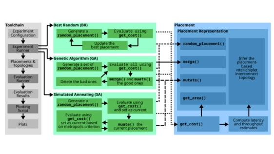
Existing approaches to maximize the performance of the ICI either optimize the placement of chiplets (with potentially heterogeneous shapes) for a predetermined ICI topology, select one topology out of a set of candidates, or they optimize the ICI topology for a 2D grid of homogeneously shaped chiplets on an active interposer. To the best of our knowledge, there is no prior work on ICI topologies for chips with heterogeneously shaped chiplets or with passive silicon interposers or silicon bridges. To fill this gap, we propose PlaceIT, a novel optimization methodology to jointly optimize the chiplet placement and ICI topology of such architectures.
The key idea is as follows: We optimize the chiplet placement without a predetermined topology. For each placement generated by an optimization algorithm, we infer a placement based ICI topology by connecting chiplets that are in close proximity in that specific placement. We then compute the latency and throughput of this combination of placement and topology for different traffic types. These latencies and throughputs together with the total chip area are used to compute a user-defined quality-score of the placement, which is returned to the optimization algorithm. Based on this quality score, the algorithm can further optimize the placement. By following this iterative process, we jointly optimize the chiplet placement and the ICI topology.
We provide our open-source framework implementing the proposed placement and topology co-optimization methodology, which we evaluate using both synthetic traffic and traffic traces. A 2D grid of chiplets with a mesh topology is used as a baseline since many proposals for 2.5D stacked chips [12], [23], [35], [17], [37] use such an architecture. We reduce the latency of synthetic L1-to-L2 and L2-to-memory traffic, the two most important traffic types for cache coherency traffic, by up to 28% and 62% respectively. For real traffic traces, we reduce the average packet latency for almost all traces and architectures considered (reduced by an 8% or 18% on average depending on the configuration of PHYs within a chiplet).
To read the full article, click here
Related Chiplet
- DPIQ Tx PICs
- IMDD Tx PICs
- Near-Packaged Optics (NPO) Chiplet Solution
- High Performance Droplet
- Interconnect Chiplet
Related Technical Papers
- FoldedHexaTorus: An Inter-Chiplet Interconnect Topology for Chiplet-based Systems using Organic and Glass Substrates
- Universal Chiplet Interconnect Express: An Open Industry Standard for Memory and Storage Applications
- High-performance, power-efficient three-dimensional system-in-package designs with universal chiplet interconnect express
- HexaMesh: Chiplet Topologies Inspired by Nature
Latest Technical Papers
- Chipmunq: Fault-Tolerant Compiler for Chiplet Quantum Architectures
- LEXI: Lossless Exponent Coding for Efficient Inter-Chiplet Communication in Hybrid LLMs
- Link Quality Aware Pathfinding for Chiplet Interconnects
- Effects of Poor Workload Partitioning on System Performance for Chiplet-Based Systems
- Mozart: Modularized and Efficient MoE Training on 3.5D Wafer-Scale Chiplet Architectures