Material-Mechanistic Interplay in SiCN Wafer Bonding for 3D Integration
By Hayato Kitagawa 1, Ryosuke Sato 1, Sodai Ebiko 1, Atsushi Nagata 2, Chiwoo Ahn 3, Yeounsoo Kim 3, Jiho Kang 3, Akira Uedono 4, Fumihiro Inoue 5
1 Yokohama National University, Japan
2 Tokyo Electron Kyushu Limited, Japan
3 SK hynix Incorporation, Japan
4 University of Tsukuba, Japan
5 Yokohama National University, Japan
Abstract
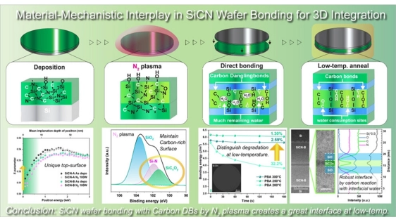
Wafer bonding is a step in processing of state-of-the-art integration architectures in CMOS devices. Sufficiently high bonding strength and low distortion with high alignment accuracy are essential to realize these device structures. A challenge in realizing advanced architectures is reducing the thermal history associated with the bonding process. Although much research has been conducted on wafer bonding methods compatible with the latest semiconductor manufacturing processes, discussions on the interface mechanisms during low temperature annealing have been insufficient. In this study, plasma-activated bonding was carried out using SiCN, which is a major bonding dielectric material. The bonding strength and water remaining at the interface were subsequently evaluated. We found that a SiCN film achieved greater bonding strength after post bond annealing at a low temperature of 250 °C and completely consumed the interfacial water. Analyses of the surface and interface revealed the carbon bonding leads to great bonding interface by low-temperature annealing.
To read the full article, click here
Related Chiplet
- DPIQ Tx PICs
- IMDD Tx PICs
- Near-Packaged Optics (NPO) Chiplet Solution
- High Performance Droplet
- Interconnect Chiplet
Related Technical Papers
- 2D materials-based 3D integration for neuromorphic hardware
- System-Technology Co-Optimization for Dense Edge Architectures using 3D Integration and Non-Volatile Memory
- Co-Optimization of Power Delivery Network Design for 3-D Heterogeneous Integration of RRAM-Based Compute In-Memory Accelerators
- Synopsys 3DIO Solution for Multi-Die Integration (2.5D/3D)
Latest Technical Papers
- Spatiotemporal thermal characterization for 3D stacked chiplet systems based on transient thermal simulation
- Interconnect-Aware Logic Resynthesis for Multi-Die FPGAs
- Scope: A Scalable Merged Pipeline Framework for Multi-Chip-Module NN Accelerators
- Scaling Routers with In-Package Optics and High-Bandwidth Memories
- TDPNavigator-Placer: Thermal- and Wirelength-Aware Chiplet Placement in 2.5D Systems Through Multi-Agent Reinforcement Learning