OPENEDGES Successfully Validated Its 7nm HBM3 Testchip
Markham, Ontario, Canada, July 15th, 2024 --- OPENEDGES Technology, Inc (OPENEDGES), the leading provider of memory subsystem IP, is pleased to announce that its subsidiary, The Six Semiconductor Inc (TSS), has successfully brought-up and validated its HBM3 testchip in 7nm process technology. The IP validation testchip and the HBM3 PHY were brought up within the first month to 6.4Gbps, and further tuning has resulted in successful operation of the HBM3 memory subsystem overclocked to 7.2Gbps.
To date, there are only a handful of IP vendors that have taped out and demonstrated HBM3 memory subsystems, as test shuttle and HBM3 DRAM die stack sample availability are both highly limited. OPENEDGES is thrilled to be amongst one of the few companies to have demonstrated an HBM3 memory subsystem in silicon.
“Our confidence in the capabilities of our highly experienced engineering team allowed us to take on the extremely challenging HBM3 PHY IP and testchip development. We are very pleased to demonstrate our excellence with the smooth and successful bring-up of our HBM3 testchip.”, said Farhad Haghighi Zadeh, TSS Principal Engineer and project lead for the HBM3 PHY and testchip.
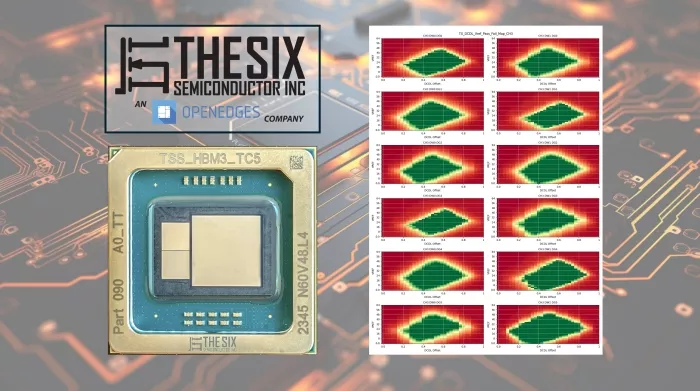
Image 1: HBM3 write schmoo for one 64-bit channel, overlayed into 12 schmoo groups at 7.2Gbps
The HBM3 PHY utilizes state-of-the-art architecture to maximize timing and voltage margins over process, voltage and temperature variations, while minimizing interruption to data traffic. The HBM3 PHY IP has the capability to support up to 16 independent and asynchronous channels, each with 2x32-bit DWORD pseudo-channels.
Additional features include fast frequency switching (multiple frequency set points), transient error handling (e.g. ECC, parity of data and command/address signals), as well as lane repair (Interconnect Redundancy Remapping), which detects, repairs, and remaps automatically in case of interconnect issues, making them transparent to the memory controller.
The development of an HBM3 memory subsystem is significantly different than that of other traditional DDR variants, as the memory controller/PHY SoC is in a 2.5D integration alongside the HBM3 die stack, the silicon interposer, and the package substrate. There is a high degree of physical architecture coherency required such that the tens of thousands of SoC micro-bumps are assigned, connected, and verified correctly. As such, it requires sophisticated design of physical constructs to carefully handle intertwined dependencies across multiple layers of design hierarchy. For example, the micro-bump array assignment would affect the PHY floorplan at the chip level, as much as it affects the RDL routings on the silicon interposer. On top of this, there is a persistent need for solid vertical delivery of power and grounds amongst a sea of signals; something that requires advanced planning—alongside the high-speed signal routings—as opposed to an afterthought.
The methodology used in the development of an HBM3 PHY testchip lend themselves very well to future chiplet designs. From the early physical planning on signal routings and power/ground deliveries, to co-planning of bumps and BGA balls along with the package substrate routings and planes, to the physical verification and cross-checks required; these are just some of the expertise and practical know-how required in the planning and development of an advanced memory subsystem chiplet.
With the silicon-proven success of its HBM3 PHY and testchip, proven design methodology and expertise, and complete portfolio of memory subsystem IPs, OPENEDGES is positioned to be the memory subsystem IP vendor of choice for the chiplet space.
“We are very proud of the successful bring-up and amazing results of our HBM3 testchip, demonstrating not just our capability to execute designs, but also to bring-up and tune the memory subsystem to maximize performance”, said Richard Fung, CEO of TSS. "With the product development philosophy of bringing the latest DDR technologies to mature technology nodes, our lineup of advanced memory subsystem IPs is the perfect fit for anyone looking to build an IO chiplet with memory interfaces. Our memory controllers and PHYs are fully integrated, fully verified, ready to be deployed in our customers' chiplet products."
“The successful validation of our HBM3 test chip is not just a milestone, but a testament to the value of our technology,” said Sean Lee, CEO of OPENEDGES Technology. “We continue to make significant progress in validating our IPs at the advanced nodes, taking further steps to empower our partners with superior performance and reliability”.
OPENEDGES is now officially listed as a chiplet ecosystem IP vendor on Chiplet Marketplace and is preparing to debut its first UCIe chiplet controller IP to the market. For more details or an exploratory discussion, please contact us at sales@openedges.com.
About OPENEDGES Technology, Inc.
OPENEDGES Technology, Inc. is a premier provider of memory subsystem IPs for the semiconductor industry. They offer a wide range of state-of-the-art solutions, including DDR memory controllers, DDR PHY, NoC interconnect, and NPU IPs that are widely adopted by customers worldwide. Their IPs comply with JEDEC standards, including LPDDR5x/5/4x/4/3, DDR5/4/3, GDDR6, and HBM3, ensuring their compatibility with the latest DDR technology trends. In 2019, they acquired The Six Semiconductor, Inc. (TSS), specializing in high-speed memory PHYs across multiple technologies. In 2021, the company established a subsidiary in the USA, followed by another in Japan in 2024, further expanding their global footprint. Additionally, ISO9001:2015 certification was achieved early this year, highlighting their commitment to quality management, and is currently undergoing the certification process for ISO26262 Automotive Safety Integrity Level (ASIL). As a publicly listed company on the Korean Stock Exchange Market (394280. KQ), OPENEDGES is well-positioned to continue its growth and maintain its leadership in the memory subsystem IPs market.
Learn more about the company and its offerings by visiting the official website at www.openedges.com.
About The Six Semiconductor Inc. (TSS)
TSS is a Canadian technology company and a wholly owned subsidiary of OPENEDGES, specializes in developing advanced high-speed DDR PHY IP solutions that cater to a wide range of applications such as AI/ML, high-performance computing (HPC), mobile devices, and automotive. The company's product portfolio includes PHY IPs for various memory standards including LPDDR5x/5/4x/4, GDDR6, and HBM3, that are optimized for power and area. TSS's solutions are designed to be compatible with multiple technologies, foundries, and process nodes. The company's team of experts have a wealth of experience in the field, and are dedicated to providing the industry with high-quality and reliable DDR PHY IP solutions. To learn more about TSS's products, visit their website at www.thesixsemi.com.
Related Chiplet
- DPIQ Tx PICs
- IMDD Tx PICs
- Near-Packaged Optics (NPO) Chiplet Solution
- High Performance Droplet
- Interconnect Chiplet
Related News
- SEMIFIVE Collaborates with OPENEDGES on Chiplet Development
- OPENEDGES Unveils UCIe Chiplet Controller IP, Expanding Design Portfolio
- Manufacturers Anticipate Completion of NVIDIA's HBM3e Verification by 1Q24; HBM4 Expected to Launch in 2026
- Signal Integrity Designs at Organic Interposer CoWoS-R for HBM3-9.2Gbps High Speed Interconnection of 2.5D-IC Chiplets Integration
Latest News
- Agileo Automation Launches Agil'EDA to Accelerate SEMI EDA Adoption for Semiconductor Equipment OEMs
- AEM and ASE Enter Strategic Partnership to Accelerate AI and HPC Test Innovation
- NLM Photonics Samples Silicon Organic Hybrid PICs Manufactured at GlobalFoundries
- Avalanche Technology and NHanced Semiconductors Leverage Advanced 2.5D Integration to Bring Optimal SWaP and Reliability to Rad-Hard FPGAs
- Open EU Foundry status granted to innovative chiplet facility