Understanding Signal Integrity in Chiplet Design

Maintaining proper signal integrity is one of the most critical considerations in chiplet design. As chipmakers push the boundaries of performance and miniaturization, ensuring clean, reliable signals between components has become more challenging than ever. For engineers navigating the complexities of signal and power integrity, understanding the nuances of these challenges is crucial for creating efficient and reliable chiplet designs.
Read more to learn about signal integrity in chiplets, its critical role in chip design, the challenges chiplets bring to the table, and how advanced tools like those offered by Cadence can redefine possibilities for engineers.
Understanding Signal Integrity in Chiplets
Signal integrity refers to the quality of the electrical signals as they travel between components in a system. For IC package designs and PCBs, maintaining signal integrity means ensuring signals remain free from degradation caused by noise, reflection, crosstalk, and losses.
Chiplets complicate this process. Unlike traditional monolithic chips, where all the components are housed on a single die, chiplets are smaller, separately manufactured components that connect to form an integrated system. While this modular approach offers significant scalability and flexibility, it also introduces new signal integrity concerns.
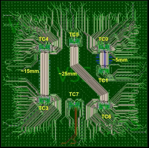
Figure 1: UCIe test package with three varying length links between chiplets
Why Signal Integrity Is Key
Maintaining reliable signal communication becomes a pivotal element in chip performance because even minor deviations in signal quality can compromise performance, increase power usage, and reduce reliability. Ensuring signal integrity guarantees high performance and safeguards your chip design's reliability and energy efficiency.
Challenges with Signal Integrity in Chiplets
- Thermal and Electrical Coupling: Given the tightly integrated nature of chiplets, thermal and electrical interactions between components become a significant consideration for maintaining power and signal integrity.
- High-Speed Data Transmission: The increased complexity of modern applications, such as AI workloads or high-bandwidth data center operations, demands faster data transfer rates. At higher frequencies, losses and reflections in the signal path become more pronounced.
- Interconnect Density: To optimize performance, interconnections between chiplets must be tightly packed. This increases the risk of crosstalk (signal interference from neighboring lines) and electromagnetic coupling.
- Complex Packaging: Chiplets often require advanced packaging technologies like 2.5D or 3D integration. These packaging solutions involve more compact designs, further heightening signal degradation risks.
- Power Delivery Noise: The intricate power delivery network (PDN) for chiplets can introduce noise into the system, impacting signal and power integrity. Ensuring low-impedance power delivery paths is essential to avoid interference.
Tools to Overcome Signal Integrity Issues
Addressing these challenges requires advanced technologies and tools capable of comprehensive signal integrity analysis. Therefore, engineers often turn to industry-leading solutions such as Cadence's Sigrity X and Clarity 3D Solver platforms.
Sigrity X
Cadence's Sigrity X Signal Integrity Analysis technology provides an integrated and powerful approach to signal and power integrity challenges, offering features such as:
- End-to-end SI/PI analysis enabling detailed, power-aware signal integrity and PDN analysis across PCB and IC package designs. It helps identify potential issues early to ensure you achieve cost, performance, and reliability goals.
- Advanced in-design interconnect modeling helps simulate signal paths and optimize impedance to reduce reflection and loss, even for tightly packed designs typical of chiplets.
- Crosstalk analysis minimizes interference risks by evaluating and mitigating crosstalk for high-density interconnections.
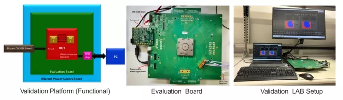
Figure 2: Cadence UCIe-Link [IP + package] chiplet-to-chiplet validation platform is used to correlate Sigrity X signal integrity simulation results
Clarity 3D Solver
Cadence's Clarity 3D Solver for High-Fidelity Analysis complements Sigrity X SI/PI by delivering 3D electromagnetic extraction capabilities for silicon, packages, and PCBs. Its benefits include:
- Analyze the coupling effects, thermal issues, and electromagnetic (EM) field behavior in package-on-package (PoP) or 2.5D/3D designs.
- Seamless integration between Clarity 3D Solver and the Cadence design ecosystem allows teams to work in a unified and efficient environment. It provides a macro and micro view for addressing signal-related challenges, helping you deliver high-performance designs within tight schedules.
Tips for Strengthening Signal Integrity in Chiplets
Beyond tooling, best practices can significantly impact your ability to maintain signal integrity. Here are actionable steps to consider:
- Adopt Power-Aware Designs: Use power-aware signal integrity analysis to account for simultaneous switching noise (SSN) and ensure robust PDNs.
- Optimize Interconnect Impedance: Maintain controlled impedance throughout the signal path to reduce reflections and minimize signal losses.
- Focus on Layout and Routing Techniques: Follow best practices for PCB layout, such as minimizing stub lengths, using proper decoupling, and separating sensitive traces from aggressive signals to mitigate crosstalk and minimize noise propagation.
- Simulate Early and Often: Simulate potential signal and power integrity issues at every stage of the design process to identify and resolve concerns early.
- Leverage Advanced Packaging: Solutions like fan-out wafer-level packaging (FOWLP) and interposers with tightly controlled design parameters can help ensure electrical and thermal stability.
Competitive Advantage with Signal Integrity
Chiplet signal integrity isn't just a technical challenge; it provides an opportunity. You can proactively manage these complexities to enable higher performance, faster time to market, and better scalability for your system. Solutions like Cadence's Sigrity X and Clarity tools empower you to confidently tackle the intricacies of chiplets while ensuring robust and reliable designs.
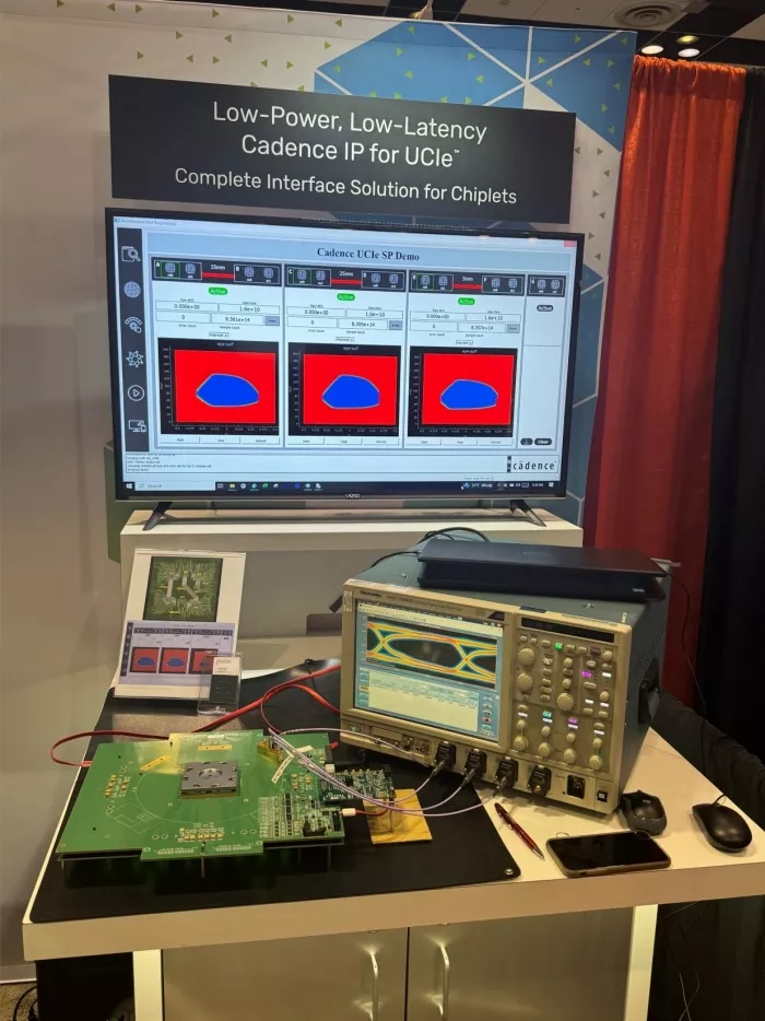
Figure 3: Cadence UCIe-Link [IP + package] chiplet-to-chiplet signal quality demonstration
Learn More About Signal Integrity
For more insights into how Cadence helps engineers solve the most complex signal integrity challenges, visit the Cadence Sigrity X Signal and Power Integrity page or read this recent article on Signal Integrity Challenges in Chiplet-Based Designs: Addressing Performance and Security.
Related Chiplet
- Interconnect Chiplet
- 12nm EURYTION RFK1 - UCIe SP based Ka-Ku Band Chiplet Transceiver
- Bridglets
- Automotive AI Accelerator
- Direct Chiplet Interface
Related Blogs
- Why Electrical Design Matters in Chiplet Architectures – Part One: Signal Integrity and Power Delivery
- Signal integrity and power integrity analysis in 3D IC design
- From Blocks to Systems: Understanding Chiplets in SoC Design
- Chiplet Integration in the Automotive Realm
Latest Blogs
- 3D-IC Market Outlook: Technology Roadmaps, Readiness, and Design Implications
- Cadence 3D-IC Success Stories: Faster Bandwidth, Lower Power, On-Time Tapeouts
- 3D-IC Test and Reliability: KGD Strategies, Access Architecture, & Failure Mode
- 3D-IC in AI, HPC, and 5G: Bandwidth, Latency, and Energy per Bit Advantages
- Bosch and the chiplet revolution: Enabling software-defined mobility