Functional Safety in a Disaggregated World

We are witnessing a dramatic rise in disaggregation and a lot of discussion around chiplet-based design. There are multiple reasons for it: as monolithic dice grow larger, they hit reticle limits and much before that the yield drops precipitously making them uneconomical. That is where monolithic designs are headed and to stay economical, they need to disaggregate into chiplets. This is not the only reason. Cost per transistor is rising in the newer process technology nodes which means it no longer makes sense to port the entire design to newer nodes as they become available. There will be portions of the design that benefit from the newer technology, and only those pieces can be ported for a more cost-effective design. Especially as the cost of large designs increases rapidly, this flexibility of a heterogenous disaggregation is key to economic viability of new SOC designs. In today’s world of high-performance designs, the trend is to go for increasingly custom silicon and the ability to amortize costs over many modular and scalable designs, is another reason to embrace chiplet-based designs.
The various chiplets in a design need a standard way of interfacing. A standard interface, such as UCIe, with significant market adoption and extensive work finalizing in detail every aspect of the connection, allows users to focus on their designs with minimal investment on interconnects, and ability to buy proven chiplets for other functions, minimizing costs and speeding up time to market, while making selections for optimizing performance, power, and cost. UCIe is a layered SerDes architecture with a PHY working with a controller to deliver packetized end-to-end communication. The subsystem includes multiple safety features, all of which must be verified to work as intended at runtime. This is referred to as functional safety (FuSa) that must be analyzed to ensure its compliance to safety standards, which brings us to the topic of safety-critical designs.
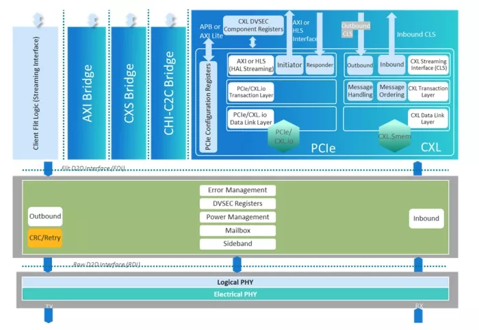
Figure 1: UCIe is a layered subsystem solution
Safety-critical designs, such as automotive designs are not immune to these considerations for moving towards disaggregated designs, and can in fact benefit from the ongoing standardization and availability of chiplets and package technologies. Many companies and consortiums are looking towards adopting chiplet technology to realize functions that form the advanced driver assistance systems (ADAS) and automated driving (AD) through the various levels.
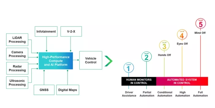
Figure 2: The various stages of vehicle automation
Safety-critical systems such as automobiles must comply with a safety standard on a system level. While no single component can make a system safety compliant, all components need to meet the requirements so that the system can comply to the safety standards. The automotive safety standard ISO 26262 has been widely adopted with four automotive safety integrity levels (ASIL), from ASIL A to ASIL D. Each ASIL level defines a maximum FIT (Failure in Time) limit. The FIT rate is the number of expected failures in 109 or a billion hours calculated using FMEDA (Failure Model Effect and Diagnostic Analysis). Along with a FIT limit, each ASIL level specifieda a SPRM (Single Pont Failure Metric), and a LFM (Latent Fault Metric) that must be met.
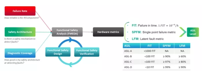
Figure 3: Key considerations and limits for ASIL levels
Designing for safety-critical application is more than just metrics, but a journey, that begins with planning which includes a safety plan and FuSa process training, design and development with robust requirements definition, tool qualification, FMEDA, DFMEA (Design Failure Mode and Effects Analysis), DFA (Dependent Failure Analysis) , generation of a safety manual, to verification, including verification plan, specification, to certification with thorough audit and assessment.
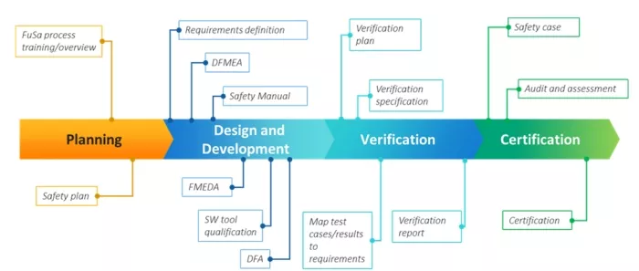
Figure 4: The various aspects of designing safety-critical components
Functional Safety manages two types of failures which may occur in a product – Random and Systematic. Random failures occur when a product, although designed correctly, eventually experience a malfunction at some point. These failures can be due to issues such as transistors or wires degrading, or external interference causing transient faults leading to temporary data processing errors. Random failures are controlled by the inclusion of Safety Mechanisms to detect when such a fault occurs. Adequate control of random failures is demonstrated through safety analysis and principally the FMEDA calculation.
Systematic failures are inherent flaws or bugs present within a product which will result in a malfunction under specific conditions. Systematic failures are introduced during the development process because of specification, design and/or implementation errors. Systematic failures are controlled by applying diligence in the processes, methods and techniques we use to specify, design, and verify the product to reduce the chances of human error letting a defect slip through. Adequate control of systematic failures is demonstrated through thorough evidence, records, and approvals at every stage of the product development process.
The process is clearly involved, and it is important to certify each component going into a safety-critical application, such as automobiles. This certification not only improves the confidence of the end user, but it also ensures metrics are accurately calculated and can be rolled up at the system level to certify the complete system. As mentioned previously, UCIe, a clear frontrunner standard connecting chiplets in a chiplet-based design, is a layered subsystem with PHY and controller working together to deliver seamless end-to-end communication. It is a SerDes-based packet protocol with data protected by CRC in the controller with robust retry mechanisms. The PHY implements multiple watchdog timers that provide diagnostics to the controller that implements bulk of the FuSa functionality.
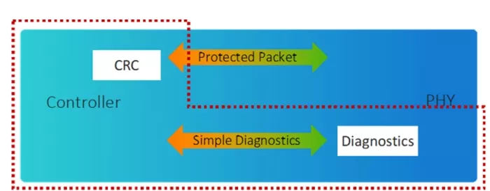
Figure 5: FuSa functionality in a SerDes such as UCIe
We are happy to announce that Cadence’s AXI-UCIe and CXS.B-UCIe controller configurations have received ISO 26262 ASIL-B certification from SGS-TÜV, part of SGS, the world’s leading testing, inspection and certification company. Our UCIe controller went through a extensive ASIL Compliant certification process with SGS-TÜV. In this process, SGS-TÜV reviewed and inspected the processes, records and outputs of our safety work on both random and systematic safety. After this thorough assessment, SSG-TÜV determined that we have addressed the relevant clauses of ISO26262 appropriately and in compliance with the requirements for an ASIL B product. SGS-TÜV issued an ASIL B Compliant certificate to provide confirmation of that conclusion to users of our UCIe controller product.
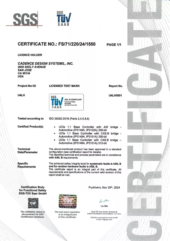
Figure 6: Certificate of ASIL-B compliance
As UCIe is a highly configurable product, 3 specific configurations and the supporting evidence of specific records of activities done directly on those 3 specific configurations have been taken through the certification process. This includes the high efficiency AXI bridge interface, providing chiplet-to-chiplet fabric extension, and multiple configurations of high efficiency CXS bridge interface, providing compute mesh network-to-network bridge connection.
This is the industry’s first UCIe IP that has achieved ISO 26262 safety compliance. This reinforces Cadence’s role as a leader in the latest interconnect protocol and chiplet IP, supporting the vision of a thriving chiplet economy, with robust standard protocols and certifications allowing our customers to de-risk their projects, when using Cadence’s groundbreaking IP and EDA tools.
Related Chiplet
- DPIQ Tx PICs
- IMDD Tx PICs
- Near-Packaged Optics (NPO) Chiplet Solution
- High Performance Droplet
- Interconnect Chiplet
Related Blogs
- Chiplets Have Become Essential in a Post-Moore's Law World
- Maximizing 3DIC Design Productivity with 3DBlox: A Look at TSMC’s Progress and Innovations in 2024
- Synopsys Aims to Reduce Silicon Design Cycles by up to a Year in Collaboration with Arm
- The Future of Faster, Smaller, and More Efficient Chips: A Breakthrough in Hybrid Bonding
Latest Blogs
- Chiplets: 8 best practices for engineering multi-die designs
- Demystifying 3D ICs: A practical framework for heterogeneous integration
- Accelerating Next-Generation EMIB-T Packaging: A Collaboration Between Synopsys and Intel Foundry
- Scoping out the chiplet-based design flow
- Understanding the Difference Between a Monolithic SoC and a Chiplet