Chiplets Are Here—And They’re Reshaping Everything

From AI to automotive, the industry has moved beyond debating chiplets to building at scale
The chiplet era is underway. Walking through Moscone Center in San Francisco recently during the 62ndDAC, one thing jumped out at me: that reality was impossible to ignore – not just in the technology demonstrations, but in the conversations happening between foundries, IP vendors, OEMs and design houses. We’ve moved from asking “if” chiplets will scale to collaboratively solving “how” we design, validate and deploy multi-vendor systems across an integrated ecosystem.
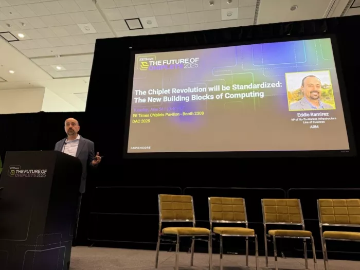
That shift in tone – from hypothetical to hands-on – was just as clear on stage at the EE Times Future of Chiplets Summit at DAC, where I had the chance to give opening remarks and, later, join a panel of industry leaders. Across both sessions, I shared what I see as the three key areas we need to focus on if we want to move chiplets from bespoke engineering projects to scalable industry practice.
The three pillars of scalable chiplet adoption
To unlock the full potential of chiplets, we must commit to three foundational imperatives:
1. Make it easy for software developers
Elegant hardware is meaningless without scalable software enablement. Specifically, software must remain stable across multiple IP generations. Developers must be able to program, provision and deploy on chiplet-based designs without complexity. That means defining common protocols, modular firmware and consistent software interfaces.
2. Build reusable silicon across the supply chain
Today, most chiplet designs are internal to a single vendor. But real scalability comes when chiplets become products – reusable, interoperable and composable across different design points and even generations. That requires deeper integration between foundries, IP vendors, packaging partners and OEMs.
3. Advance holistic system-level standards
Interfaces like UCIe have made huge strides, but they only solve part of the puzzle. System-level specifications – how chiplets communicate, boot, share memory and expose telemetry – are where true interoperability lives. That’s the vision behind Arm’s Chiplet System Architecture (CSA), now supported by over 70 partners.
AI is driving the shift: From hyperscale to edge
Why chiplets and why now? One word: AI.
AI workloads are reshaping every part of the compute stack. From data centers to automotive systems to edge devices, accelerators are taking up more real estate – and more power. As AI expands, so does the need to integrate CPUs, NPUs, GPUs, memory and IO in more flexible, efficient ways.
That’s where chiplets shine. They enable modular design, allowing compute or memory to be scaled independently, SKUs to be diversified efficiently and power/thermal budgets to be optimized more granularly. For smaller players, this opens the door to entering complex markets without monolithic SoC investments.
And through Arm KleidiAI, we ensure that developers can run inference on a consistent AI software stack – from the cloud to the Raspberry Pi – across diverse hardware implementations.
Ecosystem engineering: Total Design and Project Leapfrog
To make chiplets viable at scale, the industry needs more than good specs; it needs coordinated execution. That shared imperative was the impetus behind the creation of Arm Total Design, a partner program uniting foundries, design houses, IP vendors, EDA providers and OEMs to accelerate the creation of interoperable, silicon-proven chiplets.
One of the most exciting outcomes of this collaboration is Project Leapfrog.
Leapfrog is an ambitious multi-vendor initiative to build a chiplet-based AI training platform designed to rival monolithic architectures like NVIDIA’s GB200 – only more efficient, scalable and open.
Here’s a closer look at what’s under the hood:
- Compute Subsystem: Built on Arm Neoverse cores using our Compute Subsystem (CSS), ADTechnology is delivering a 64-core chiplet ready for AI-intensive workloads.
- AI Accelerator: Rebellions contributes a high-performance accelerator chiplet optimized for deep learning training and inference.
- Fabric Chiplet: Interconnect logic that links the compute and AI engines efficiently within the package.
- Memory and IO: HBM-based memory subsystems and cutting-edge IO are integrated via advanced UCIe links.
- Packaging and Process: Manufactured using Samsung Foundry’s leading-edge 3nm/4nm nodes and 2.5D I-Cube packaging.
What makes Leapfrog unique isn’t just the hardware; it’s the collaboration model. This is a first-of-its-kind demonstration that industry-leading performance can come from modular, multi-vendor chiplets, not just vertically integrated SoCs. Early testing suggests Leapfrog will achieve 3x the power efficiency of conventional GPU-based AI training systems.
This is what the future looks like: specialized silicon, shared innovation and composable performance at scale.
Standards, software and the road ahead
While hardware is advancing, the industry’s biggest bottleneck may be the software and system integration layer. Chiplet-based designs require new approaches to:
- Secure boot and telemetry across disaggregated components
- Debugging across chiplet boundaries
- Firmware modularity and platform enablement
- System-level validation pre-silicon
That’s why we developed the Arm CSA specification (mentioned earlier), which we released earlier this year. With more than 70 partners involved, the CSA addresses everything from security and telemetry interfaces to firmware boot sequences and coherent accelerator integration. We’ve created profiles for different use cases—compute-to-accelerator, I/O-based designs—each with fully specified interfaces and protocols.
The response has been encouraging. Since launch, we’ve seen significant interest in expanding CSA for security implementations, confidential computing and low-latency real-time systems for automotive and aerospace applications.
We’re also partnering with EDA leaders like Synopsys, Cadence and Siemens to develop pre-silicon modeling, co-verification and emulation environments that make chiplet-based systems just as robust as monolithic ones.
And perhaps most promising: OEMs are beginning to issue RFIs for chiplets, not just SoCs – a sign that the marketplace mindset is taking root.
Where we’re headed
In five years, I expect most product companies – whether in cloud, automotive, mobile, or industrial – will be deploying some form of customized silicon. Chiplets make that possible. They’re not just a packaging solution – they’re a strategic enabler for power efficiency, performance differentiation and time-to-market advantage.
But we won’t get there alone.
The chiplet economy depends on a collective vision: composable systems, interoperable products and common language across companies. At Arm, we’re committed to enabling that future through open standards, scalable IP and real-world partnerships like Leapfrog.
We’re no longer imagining the future of computing – we’re building it. Chip by chip.
Related Chiplet
- Interconnect Chiplet
- 12nm EURYTION RFK1 - UCIe SP based Ka-Ku Band Chiplet Transceiver
- Bridglets
- Automotive AI Accelerator
- Direct Chiplet Interface
Related Blogs
- Chiplets Turn 10: Here are Ten Things to Know
- What are chiplets?
- What are Chiplets and how they Assemble Into the Most Advanced SoCs
- The Automotive Industry's Next Leap: Why Chiplets Are the Fuel for Innovation
Latest Blogs
- Advancing Europe’s Automotive Chiplet Vision: Arteris Joins CHASSIS to Accelerate Software-Defined Mobility
- 3D-IC Market Outlook: Technology Roadmaps, Readiness, and Design Implications
- Cadence 3D-IC Success Stories: Faster Bandwidth, Lower Power, On-Time Tapeouts
- 3D-IC Test and Reliability: KGD Strategies, Access Architecture, & Failure Mode
- 3D-IC in AI, HPC, and 5G: Bandwidth, Latency, and Energy per Bit Advantages