Testing At The Speed Of Light: Enabling Scalable Optical Testing For Silicon Photonics And CPO

Growing adoption of optical interconnects in data centers necessitates high-volume, automated test solutions.
Today, a single ChatGPT query consumes roughly ten times more power than a traditional Google search and will only continue to grow as AI extends to image and video generation. With this growth not only in AI, but also in cloud computing and high-performance computing (HPC), data center electricity consumption is projected to account for up to 9.1% of total U.S. electricity use by 2030.
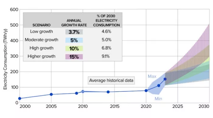
Fig. 1: Projections of potential electricity consumption by U.S. data centers: 2023-2030. (Source: EPRI)
This surge in power consumption is driving major chip designers to invest in optical interconnect solutions, particularly silicon photonics (SiPh) and co-packaged optics (CPO), to reduce energy usage. Broadcom reported a 30% power savings with its first co-packaged optics switch, while NVIDIA recently unveiled a CPO switch offering 3.5x energy efficiency compared to traditional pluggable transceivers.
Silicon photonics and co-packaged optics: A new era of connectivity
Silicon photonics leverages silicon to create photonic integrated circuits (PICs), which include optical modulators, photodetectors, and waveguides. These are fabricated using mature CMOS process nodes (65nm or higher), enabling faster data transfer (200G+ vs. <100G with InP or GaAs), lower power consumption, and greater bandwidth—ideal for data center and telecom applications.
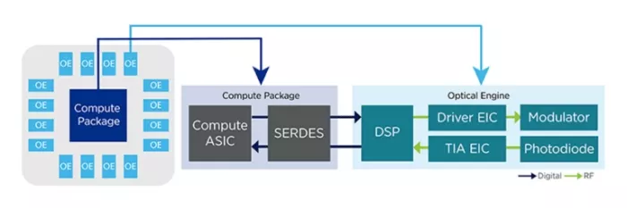
Fig. 2: Co-packaged optics with 16 Optical Engines.
Co-packaged optics (CPO) integrate optical transceivers (optical engines) directly with HPC devices—such as network switches, GPUs, or AI accelerators—within a single package. This architecture eliminates slower, power-hungry copper links by replacing them with fiber optics, improving bandwidth density, power efficiency, and latency. Industry leaders including NVIDIA, Broadcom, Marvell, AMD, and IBM have all announced CPO product developments in the past year.
However, the adoption of SiPh and CPO introduces new optical test challenges that must be addressed with scalable, high-volume manufacturing solutions.
Key challenges in co-packaged optics testing
Testing CPO devices involves multiple stages, beginning with wafer-level testing of photonic integrated circuits. The primary challenge here is achieving sub-micrometer precision in fiber alignment. Optical fibers—connected to lasers and power meters—must be aligned with extreme accuracy to on-wafer optical couplers. In contrast, most electrical probers today only achieve alignment within tens of micrometers. This precision is critical for accurate power measurements and wavelength-specific responsiveness.
After singulation, the photonic IC must be tested again before integration into a co-packaged device. This may involve testing in bare die form or after partial packaging. Devices may include optical connectors for passive alignment or require active fiber alignment. The lack of connector standardization further complicates automation, requiring test systems to support a variety of connector types.
High-speed or “at-speed” testing is also essential. Some devices feature built-in self-test capabilities, generating data at 112 Gbps or 224 Gbps PAM4. These require optical loopback from TX to RX ports. Others demand external high-speed oscilloscopes and bit error rate testers to validate performance.
Finally, once optical engines are co-packaged with a network ASIC, GPU, or AI accelerator, the entire package must be tested. Current CPO designs include 4 to 36 optical engines across 2 to 4 sides of a compute die. Automated test systems must establish optical connections on all sides, provide high-power lasers, enable optical loopback for mission-mode testing, and manage thermal loads of several thousand watts.
Scaling to high-volume manufacturing
Solving these challenges at the prototype stage is not enough. While pluggable transceivers currently ship 5–10 million units annually, CPO adoption could push optical engine volumes into the tens or hundreds of millions. Manual or semi-custom testing methods won’t scale.
To meet this demand, optical instruments and alignment systems must be integrated into thousands of automated semiconductor test cells that seamlessly interface with foundry and OSAT infrastructure. These “optoelectronic” test cells must be user-friendly for operators and support staff—not just optical engineers. High-volume, automated test solutions are essential to unlocking the full potential of SiPh and CPO technologies—delivering lower power consumption and higher bandwidth in next-generation data centers.
Optical test innovation
Teradyne is at the forefront of developing test solutions for every stage of the SiPh and CPO lifecycle—from wafer-level to co-packaged device testing, across ATE, SLT, and board-level platforms. Teradyne recently introduced the first production solution for double-sided wafer probe testing of silicon photonics, streamlining both electrical and optical test processes. Teradyne also acquired Quantifi Photonics to expand its portfolio with high-channel-count, flexible optical test instrumentation. By combining deep electrical test expertise with cutting-edge optical capabilities, Teradyne is accelerating the adoption of silicon photonics and co-packaged optics in AI and HPC—at the speed of light.
Related Chiplet
- Interconnect Chiplet
- 12nm EURYTION RFK1 - UCIe SP based Ka-Ku Band Chiplet Transceiver
- Bridglets
- Automotive AI Accelerator
- Direct Chiplet Interface
Related Blogs
- AMI Outlines Full Support for Arm Total Design Chiplet Architecture to Custom Silicon Designers and Producers at APAC ATD Summit
- Advanced Packaging Evolution: Chiplet and Silicon Photonics-CPO
- How Disruptive will Chiplets be for Intel and TSMC?
- Podcast: How Achronix is Enabling Multi-Die Design and a Chiplet Ecosystem with Nick Ilyadis
Latest Blogs
- 3D-IC Market Outlook: Technology Roadmaps, Readiness, and Design Implications
- Cadence 3D-IC Success Stories: Faster Bandwidth, Lower Power, On-Time Tapeouts
- 3D-IC Test and Reliability: KGD Strategies, Access Architecture, & Failure Mode
- 3D-IC in AI, HPC, and 5G: Bandwidth, Latency, and Energy per Bit Advantages
- Bosch and the chiplet revolution: Enabling software-defined mobility