3D-IC Test and Reliability: KGD Strategies, Access Architecture, & Failure Mode

3D-IC technology is redefining how advanced systems are built, but it also introduces a new class of challenges in 3D-IC testing and reliability. As multi-die and chiplet-based systems replace monolithic SoCs, achieving predictable yield, comprehensive test coverage, and long-term lifecycle reliability become as critical as meeting performance and power targets. Known good die (KGD) strategies, standardized die-to-die test access, and vertical reliability modeling are no longer optional optimizations; they are foundational requirements for scalable 3D-IC deployment.

Unlike traditional planar designs, 3D-IC test and reliability planning must account for stacked manufacturing flows, wafer thinning and bonding operations, limited post-assembly access, and tightly coupled electrical, thermal, and mechanical interactions. These constraints fundamentally change how test insertion, yield learning, and failure analysis are approached. This blog post examines the core test strategies, reliability risks, and lifecycle considerations that shape modern multi-die validation, from early architecture through high-volume manufacturing.
Known Good Die (KGD) and Yield Management
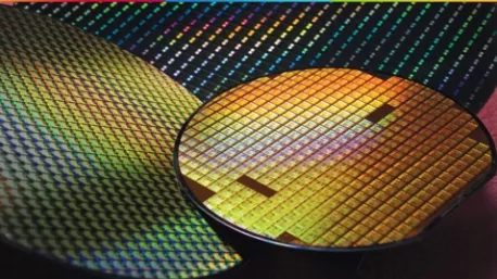
The economic viability of 3D-ICs hinges on the ability to assemble only KGD. Once chiplets are stacked using micro-bumps or hybrid bonding, the ability to rework is extremely limited, and a single defective die can render an entire package unusable. As a result, KGD testing is a central pillar of yield management in 3D-IC technology, particularly for high-cost AI and HPC packages.
Pre-Bond Test Limitations
Achieving true KGD status is more complex than in a traditional wafer test. Wafer-level probing for chiplets must contend with:
- Limited probe power delivery and reduced noise margins
- Restricted thermal coverage for hot and cold testing conditions
- Die-to-die interfaces (e.g., UCIe or proprietary links) that are not designed to directly drive external test equipment
Because of these limitations, KGD strategies typically rely on a carefully balanced combination of structural test, parametric screening, and built-in self-test (BIST) rather than full functional coverage at wafer sort. Pre-bond and post-bond test flows must be co-optimized to maximize defect detection before stacking.
Yield Amplification Risk
Yield loss in stacked designs is multiplicative. Latent defects in TSVs, micro-bumps, or hybrid bonding interfaces may not manifest until after stacking or reflow, dramatically amplifying cost impact. This reinforces the industry’s well-known “rule of ten” economics: Detecting defects as early as possible reduces downstream cost by an order of magnitude at each stage.
Cadence’s Integrity 3D-IC Platform supports yield-aware planning by enabling early analysis of interconnect density, TSV placement, power delivery paths, and thermal constraints—helping teams design stacks that are inherently more testable, manufacturable, and resilient to yield loss.
Die-to-Die Link Testing and Access Standards
Testing of 3D-IC technology does not stop at individual dies. Die-to-die interconnect testing is essential for validating signal integrity, continuity, and performance of vertical and lateral links once dies are assembled, particularly for high-speed chiplet interfaces.
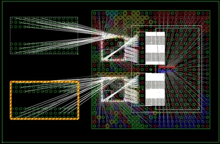
IEEE 1838 and Standardized Test Access
The IEEE 1838 standard defines a scalable test access architecture for stacked dies, introducing:
- Die wrappers to isolate individual dies during test
- A serial control mechanism for accessing embedded test logic
- Optional flexible parallel ports for higher test bandwidth
The standard works in concert with the IEEE 1149.1 (boundary scan) and IEEE 1687 (IJTAG) standards, enabling structured DFT for multi-die systems while maintaining compatibility with existing test infrastructure. This approach is increasingly relevant for UCIe-based die-to-die links, where standardized access is critical for interoperability and yield learning.
Access Architecture Implications
In 3D-ICs, test access architecture must be planned alongside physical and package design. Decisions around wrapper placement, access routing, and test bandwidth directly affect routing congestion, power integrity (PI), and thermal behavior. Post-assembly test, therefore, becomes a system-level tradeoff, not a back-end afterthought.
Cadence’s system-aware design environment allows architects to evaluate test access feasibility early, aligning DFT strategies with package routing, interposer constraints, and die-to-die signaling requirements.
Thermo-Mechanical Stress, Warpage, and CTE Issues
Reliability challenges in 3D-IC technology extend well beyond electrical behavior. Thermo-mechanical stress arises from the interaction of dissimilar materials under temperature cycling during wafer thinning, bonding, reflow, and real-world operation.
Stress Drivers in Stacked Designs
Key contributors include:
- Coefficient of thermal expansion (CTE) mismatch between silicon, copper TSVs, underfill, and substrates
- Wafer thinning and bonding-induced residual stress
- Non-uniform power dissipation across stacked dies
These effects can result in warpage in stacked dies, die cracking, delamination, and fatigue failure in solder joints, TSVs, or hybrid bonds—directly impacting long-term reliability.
Design-Time Mitigation
Addressing the mechanical reliability requires early modeling and layout optimization, including:
- TSV and bump placement optimization to balance stress distribution
- Selection of low-CTE underfill and bonding materials
- Substrate thickness, stack height, and assembly tradeoff analysis
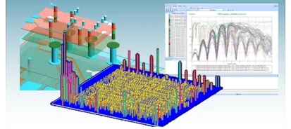
Multiphysics simulation—combining thermal, mechanical, and electrical analysis—is essential for predicting failure risk before silicon fabrication. Cadence workflows support this co-analysis approach, enabling teams to identify high-risk regions early and refine stack architecture accordingly.
EM/PI Risk in Vertical Current Paths
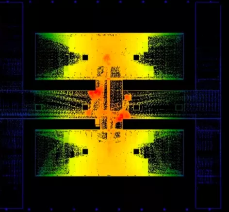
As power density increases, electromigration (EM) and power integrity challenges become more severe in 3D-ICs, particularly in vertical current paths supporting AI accelerators and high-performance compute workloads.
Vertical Power Delivery Challenges
High current density through TSVs, micro-bumps, and hybrid bonds increases susceptibility to:
- Electromigration-induced voiding
- IR drop and localized power rail collapse
- Ground bounce and coupling noise between adjacent vertical structures
Unlike planar designs, failures in vertical interconnects can compromise multiple dies simultaneously, accelerating system-level failure.
EM/PI Analysis as a Reliability Requirement
Preventing EM risk in TSVs and hybrid bonding requires accurate modeling of current density, temperature coupling, and material limits under realistic operating conditions. Cadence’s SI/PI and EM analysis capabilities, integrated with the Integrity 3D-IC Platform, enable designers to assess vertical current path reliability using physics-based models rather than idealized assumptions.
Reliability Planning Across Lifecycle and Environments
True 3D-IC reliability across the product lifecycle cannot rely solely on standard qualification tests. The combination of new materials, interfaces, and assembly flows demands a physics-based, mission-profile-driven approach.
Physics of Failure and Accelerated Stress
Physics of failure (PoF) methodologies help teams understand how failure mechanisms evolve over time due to thermal cycling, mechanical stress, humidity, and electrical load. Reliability enhancement testing (RET) pushes devices beyond nominal limits to expose weaknesses early, an approach that is especially critical for automotive, aerospace, and industrial applications.
Continuous Reliability Awareness
Reliability planning must span:
- Architecture and design decisions
- Manufacturing process windows
- Real-world operating and mission profiles
Cadence solutions support this continuity by linking system-level analysis with detailed implementation data, ensuring reliability assumptions remain valid from concept through deployment.
Production Ramp Considerations for Stacked Designs
Scaling 3D-ICs from prototype to high-volume manufacturing (HVM) introduces additional constraints.
Key production ramp considerations include:
- Tight process control for wafer thinning, alignment, bonding, and reflow
- Predictable supply of high-quality KGD across vendors
- Automation of DFT insertion, test generation, and validation to manage complexity
Test cost optimization for 3D-ICs becomes increasingly important as stack complexity increases. Integrating test planning and reliability analysis early helps prevent yield surprises that can delay or derail production ramps.
Reliability Is the Enabler of Scalable 3D-IC Systems
As 3D-IC technology becomes mainstream, 3D-IC testing and reliability are no longer downstream concerns—they are architectural requirements. Robust KGD strategies, standardized die-to-die access, and manufacturing-aware multiphysics analysis are essential to achieving high-yield, manufacturable, and long-lived multi-die systems.
Cadence’s Integrity 3D-IC Platform, together with Clarity 3D Solver and system-level SI/PI/EM analysis solutions, provides a unified framework for addressing test and reliability from concept through production. By enabling early visibility into failure modes, yield risk, and lifecycle behavior, Cadence helps teams confidently scale advanced packaging innovations into real-world systems.
In the era of chiplets and heterogeneous integration, reliability is not a constraint—it is the foundation that makes 3D-IC success possible.
Request a Design Assessment or Demo
If your team is exploring 3D-IC integration, you can request a design assessment to evaluate stack feasibility, interposer requirements, and potential multiphysics risk areas. This collaborative review helps identify where Cadence solutions can improve integration efficiency, modeling accuracy, and time to signoff.
Explore Cadence’s 3D-IC ecosystem:
- Cadence Multi-Die 3D-IC Solution to see how Cadence empowers next-generation system innovation.
- Integrity 3D-IC Platform to discover how 3D design and signoff enable system-level optimization.
- Allegro X Advanced Package Designer Platform to accelerate system performance and seamless integration.
- Celsius Thermal Solver enables 3D-IC thermal planning and signoff.
Talk to a 3D-IC Specialist to discuss your design challenges and roadmap.
Related Chiplet
- DPIQ Tx PICs
- IMDD Tx PICs
- Near-Packaged Optics (NPO) Chiplet Solution
- High Performance Droplet
- Interconnect Chiplet
Related Blogs
- Synopsys and Intel Team Up on the First UCIe-Connected Chiplet-Based Test Chip
- Maximizing 3DIC Design Productivity with 3DBlox: A Look at TSMC’s Progress and Innovations in 2024
- Industry Standards for Chiplets and Their Role In Test
- Multi-Die Health and Reliability: Synopsys and TSMC Showcase UCIe Advances
Latest Blogs
- UCIe Full Signal Integrity Analysis Flow
- From horsepower to high-performance compute: automotive chiplets take the leap towards autonomous edge computing
- Designing the Future We Can Verify: A Vision for Multi-Die Design, STCO, and Trustworthy AI
- Wafer-Scale vs. Chiplets: The new war? - Part 2: Two Paths, One Wall
- Wafer-Scale vs. Chiplets: The new war?