Cadence 3D-IC Success Stories: Faster Bandwidth, Lower Power, On-Time Tapeouts

As scaling at advanced nodes becomes increasingly constrained by cost, yield, and power density, semiconductor innovation is shifting decisively toward 3D-IC technologies, chiplets, and heterogeneous integration. Across AI infrastructure, cloud computing, automotive electronics, and high-performance systems, design teams are moving beyond monolithic SoCs to unlock new levels of performance, efficiency, and scalability through advanced packaging.
What separates successful programs from stalled initiatives is not packaging ambition alone, but manufacturing-aware system design, where dies, interposers, packages, and analysis are treated as a single, coherent system from the earliest planning stages.
This blog aggregates Cadence 3D-IC case studies drawn from real-world production deployments. These examples highlight measurable outcomes in bandwidth, power efficiency, reliability, and tapeout predictability, demonstrating how Cadence enables repeatable 3D-IC tapeout success at scale.
Scaling Next-Generation AI ASICs with 3.5D Integration
Within the AI and machine learning (ML) accelerator space, the rapid rise of large language models (LLMs) and deep learning recommendation models (DLRMs) has created unprecedented demands for memory bandwidth and compute density. To address these requirements, AI ASICs have evolved from large, monolithic dies toward heterogeneous chiplet architectures enabled by advanced packaging technologies.
A leading infrastructure silicon provider represents a growing class of 3D-IC implementation examples often referred to as "3.5D" integration. This approach combines large reticle-scale logic dies, 2.5D interposers, and selective 3D die stacking to achieve architectural scalability. While powerful, these designs introduce significant challenges in floorplanning, assembly correctness, and cross-die connectivity.
Using the Cadence Integrity 3D-IC Platform, the design team implemented a correct-by-construction floorplanning and assembly methodology that preserved system intent across dies and package structures. Instead of relying on fragmented tool handoffs, the platform enabled early stack planning, deterministic connectivity definition, and continuous validation throughout the construction process.
The result was first-time-right ASIC silicon—a critical requirement for large-scale AI accelerators, where respins carry substantial cost and schedule risk. This example illustrates how Cadence 3D-IC solutions are increasingly defined by predictability and manufacturing readiness, not just peak performance.
Integrated System Verification for Large-Scale Chiplet Designs
Cloud-scale workloads place sustained pressure on chiplet-based system architectures, demanding high performance alongside aggressive deployment timelines. In advanced multi-die compute platforms developed by a major cloud and platform provider, modular chiplets improved scalability, but also introduced added complexity in system planning, verification, and signoff.
One of the most persistent challenges in traditional flows is the loss of system intent when flattened GDS data is transferred into downstream system analysis tools. Polygon abstraction, translation errors, and disconnected verification steps often lead to false signal integrity (SI) and power integrity (PI) violations, which extend analysis cycles and slow down the design closure process.
The methodology significantly improved productivity during chiplet assembly and reduced overall time to analysis, reinforcing the importance of EDA integration in enabling successful and scalable heterogeneous integration.
This customer deployment demonstrates how Cadence 3D-IC design methodologies benefit from tightly integrated planning and analysis. Using the Integrity 3D-IC Platform, multi-chiplet construction, SI, and PI analysis were performed within a unified, in-design environment. Direct cut-in-construct analysis eliminated translation artifacts and enabled results to be back-annotated directly into the physical implementation.
The approach significantly improved productivity during chiplet assembly and reduced overall time to analysis, reinforcing the importance of EDA integration in scalable heterogeneous integration workflows.
Scalable Power Integrity for Advanced 3D-IC Architectures
As 3D-IC architecture continues to grow in complexity, power delivery networks (PDNs) have emerged as a dominant design risk. Vertical stacking, dense microbump arrays, and multi-die interactions reveal the limitations of traditional 2D power integrity methodologies, particularly at advanced nodes.
Advanced packaging case studies from a leading semiconductor manufacturer illustrate how Cadence enables manufacturing-ready 3D-IC solutions through scalable power integrity analysis. By leveraging the Voltus IC Power Integrity Solution, Innovus Implementation System, and the Integrity 3D-IC Platform, the design team implemented a comprehensive PI methodology spanning early exploration through final signoff.
Two techniques proved especially impactful. Adaptive partitioning grouped dies with similar spatial characteristics, reducing unnecessary simulation iterations and improving convergence. And XM-based hierarchical modeling enabled high-accuracy macro abstractions that dramatically reduced EM-IR simulation turnaround time while maintaining signoff-level accuracy.
In an advanced 2.5D design with approximately 100K bumps, the EM-IR turnaround time was reduced by more than 10% with minimal impact on accuracy. In larger hierarchical designs, simulation time dropped by over 50%, with power and ground node counts reduced from billions to tractable levels. These results underscore how Cadence 3D-IC design outcomes are increasingly defined by productivity, scalability, and reliability, rather than performance alone.
Foundry-Aligned 3D-IC Manufacturing Flows for High-Volume Manufacturing
Beyond individual successful customer deployments, Cadence's 3D-IC ecosystem strength is reinforced by deep, ongoing alignment with leading semiconductor foundries. Through close foundry collaborations, Cadence delivers production-proven 3D-IC design flows that are certified, validated, and explicitly engineered for manufacturing readiness—not just design feasibility.
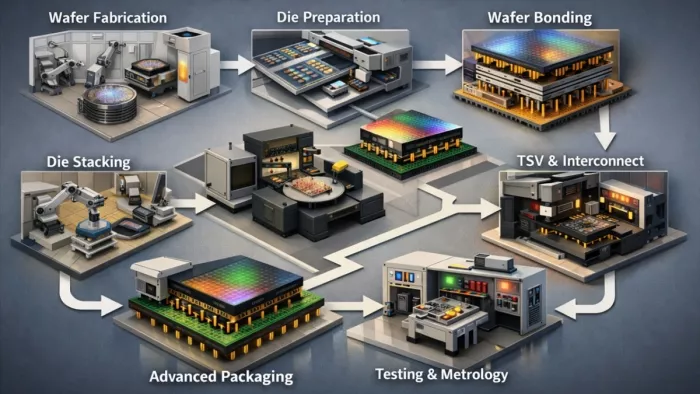
Representative visualization of scalable 3D-IC manufacturing workflows
The Cadence Multi-Die 3D-IC Solution supports a wide range of advanced integration technologies, including complex die stacking configurations, hybrid bonding, silicon and organic interposers, and emerging foundry-specific packaging innovations. These capabilities are tightly integrated with Clarity 3D Solver, Sigrity X Platform, Celsius Thermal Solver, and Voltus IC Power Integrity Solution, enabling system-level SI, PI, thermal, and reliability analysis throughout the design cycle.
By embedding foundry requirements directly into the 3D-IC workflow, this foundry-qualified approach enables design teams to transition from architecture exploration to tapeout with greater confidence, thereby reducing risk across wafer stacking, interposer implementation, and package-aware signoff for high-volume production environments.
What These 3D-IC Success Stories Reveal
Across these Cadence 3D-IC case studies, several consistent themes emerge:
- Successful 3D-IC programs treat the package as a first-class design object
- Early, integrated multiphysics analysis is essential to reduce respins
- Hierarchical and partitioned methodologies are critical for scalability
- Manufacturing awareness must be embedded, not added late
These lessons directly address common industry questions, including challenges in 3D-IC implementation, strategies to reduce power in 3D-IC designs, and the role of EDA in enabling reliable heterogeneous integration.
Scaling Repeatable 3D-IC Tapeout Success with Cadence
As heterogeneous integration becomes the foundation of next-generation systems, design success depends on more than innovative architectures. It requires repeatable, manufacturing-ready workflows that scale across products, nodes, and markets.
The Cadence Integrity 3D-IC Platform, combined with industry-leading system, power, signal, and thermal analysis, enables teams to move from concept to silicon with confidence. Together, these Cadence 3D-IC success stories demonstrate not isolated wins, but a scalable methodology for delivering faster bandwidth, lower power, and predictable tapeouts in the era of advanced packaging.
Request a Design Assessment or Demo
If your team is exploring 3D-IC integration, you can request a design assessment to evaluate stack feasibility, interposer requirements, and potential multiphysics risk areas. This collaborative review helps identify where Cadence solutions can improve integration efficiency, modeling accuracy, and time to signoff.
Explore Cadence's 3D-IC ecosystem:
- Cadence Multi-Die 3D-IC Solution to see how Cadence empowers next-generation system innovation.
- Integrity 3D-IC Platform to discover how 3D design and signoff enable system-level optimization.
- Allegro X Advanced Package Designer Platform to accelerate system performance and seamless integration.
- Celsius Thermal Solver enables 3D-IC thermal planning and signoff.
Talk to a 3D-IC Specialist to discuss your design challenges and roadmap.
Related Chiplet
- Interconnect Chiplet
- 12nm EURYTION RFK1 - UCIe SP based Ka-Ku Band Chiplet Transceiver
- Bridglets
- Automotive AI Accelerator
- Direct Chiplet Interface
Related Blogs
- How Cadence Is Expanding Innovation for 3D-IC Design
- Using Voltus IC Power Integrity to Overcome 3D-IC Design Challenges
- Cadence Collaborates with TSMC to Shape the Future of 3D-IC
- Cadence Recognized for Accelerating AI and 3D-IC Applications by Samsung Foundry
Latest Blogs
- 3D-IC Market Outlook: Technology Roadmaps, Readiness, and Design Implications
- Cadence 3D-IC Success Stories: Faster Bandwidth, Lower Power, On-Time Tapeouts
- 3D-IC Test and Reliability: KGD Strategies, Access Architecture, & Failure Mode
- 3D-IC in AI, HPC, and 5G: Bandwidth, Latency, and Energy per Bit Advantages
- Bosch and the chiplet revolution: Enabling software-defined mobility