2.5D vs 3D-IC: Architecture Tradeoffs, and a Practical Selection

As traditional scaling slows and multi-die integration becomes the new engine of semiconductor performance, the question facing every system architect is no longer whether to adopt advanced packaging, but which architecture to choose. The decision between 2.5D and 3D-IC now shapes achievable bandwidth, energy efficiency, thermal limits, system size, and even program schedules. And with AI and high-performance computing (HPC) workloads pushing die-to-die bandwidth into multi-terabyte-per-second territory, choosing the right integration path has never been more critical.
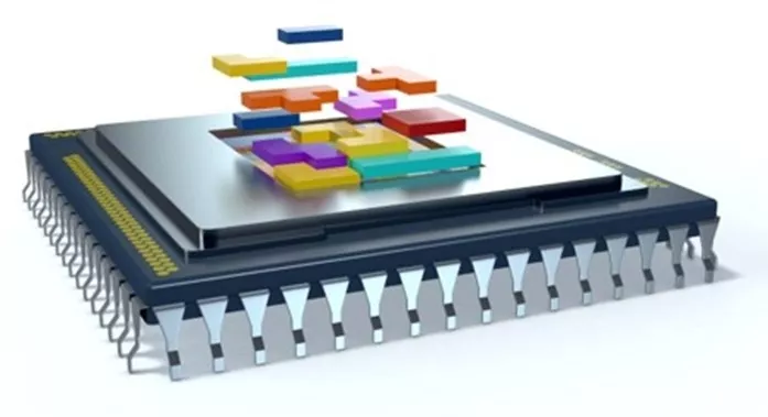
Both 2.5D and 3D-IC integrate multiple dies in a single package, but they do so in fundamentally different ways. This blog provides technically grounded comparisons to help select the right architecture based on performance goals, thermal constraints, manufacturability, and cost.
2.5D Integration: Side-By-Side on an Interposer
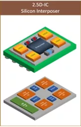 In 2.5D integration, active dies such as logic chiplets, I/O dies, or high-bandwidth memory (HBM) stacks are placed horizontally on a silicon interposer. The interposer provides dense wiring through fine-pitch redistribution layers (RDLs), while through-silicon vias (TSVs) connect it down to the package substrate.
This architecture delivers significantly higher interconnect density than conventional 2D packaging, while maintaining:
- Predictable thermal performance due to wide-area horizontal heat spreading
- Heterogeneous integration, enabling chiplets from different process nodes or foundries
- Support for very large dies, including those exceeding reticle limits
- Lower design, test, and manufacturing risk compared to full 3D stacks
- A mature, scalable supply chain, especially for HBM-based architecture
These strengths have made 2.5D the dominant platform for HPC processors, large networking ASICs, and today's AI accelerators.
3D-IC: Vertical Stacking for Maximum Density
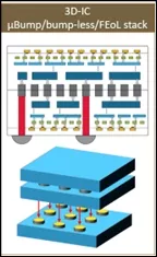 3D-IC architectures take integration further by vertically stacking dies and connecting them using TSVs or hybrid bonding. These extremely short vertical links reduce interconnect length by an order of magnitude or more, enabling new classes of performance:
- Maximum bandwidth density
- Ultra-low latency, ideal for tightly coupled compute-memory paths
- Exceptional energy efficiency due to reduced interconnect power
However, 3D stacking introduces several challenges: thermal hotspots become more difficult to manage as heat sources are vertically aligned, testing and characterization are more complex once dies are bonded, and manufacturing complexity and cost increase due to TSV fabrication, alignment accuracy, and bonding steps. Despite these challenges, 3D-IC is experiencing accelerated adoption, particularly in logic-under-memory stacks, compact edge devices, low-power compute modules, and as replacements for next-generation HBM.
Decision Framework for Your Program Constraints
Choosing between 2.5D and 3D-IC depends on your project's priorities: performance, thermals, cost, manufacturability, and schedule risk. Below is a practical guide for decision-makers.
2.5D vs 3D-IC: Technical Comparison
|
Aspect |
2.5D Packaging |
3D-IC Packaging |
|
Bandwidth |
Very high via interposer RDLs |
Highest via short TSVs |
|
Latency |
Low; higher than 3D |
Minimal |
|
Power Efficiency |
Strong, heterogeneous nodes |
Exceptional |
|
Thermals |
Easier heat dissipation |
Difficult, stacked hotspots |
|
Testing |
Mature, pre-bond testable |
Complex, limited access |
|
Cost |
High (interposer), but good yields |
Highest—TSVs + bonding steps |
|
Schedule Risk |
Moderate |
High |
|
Form Factor |
Larger footprint |
Ultra-compact |
When to Choose 2.5D Technology
Select 2.5D if your program requires:
- Enhanced thermal management with effective heat dissipation
- HBM-class bandwidth without the high risks associated with 3D stacking
- Simpler design and manufacturing processes
- Heterogeneous integration of various nodes and intellectual property sources
- Predictable costs and quicker time-to-market
2.5D technology is ideal for applications such as AI accelerators, reticle-limited compute dies, networking ASICs, high-performance computing (HPC) nodes, and chiplet-based architectures that scale horizontally rather than vertically.
When to Choose 3D-IC Technology
Opt for 3D-IC if your objectives include:
- Maximum bandwidth with minimal latency, such as placing logic beneath cache or stacked memory
- A compact footprint suitable for edge computing, augmented reality/virtual reality (AR/VR), and mobile system on chips (SoCs)
- Power efficiency improvements achieved through short vertical interconnects
- Architectural innovations resulting from vertical partitioning
3D-IC technology is gaining popularity for applications like 3D-stacked DRAM replacements, high-density memory fabrics, vertical compute subsystems, and emerging AI architectures (e.g., integrating logic with near-memory compute). As hybrid bonding and ultra-fine pitch TSVs advance, 3D-IC will increasingly penetrate mainstream compute designs.
Tool Flows for Architectural Exploration
As integration grows more complex, EDA workflows must unify the way teams plan, assemble, analyze, and sign off on multi-die systems. The Cadence Integrity 3D-IC Platform addresses these needs with:
- System-level architecture exploration and floorplanning
- Package-aware parasitic extraction
- Thermal and structural analysis
- Signal and power integrity co-analysis
- Multi-die assembly checks and verification
- Co-simulation across dies, interposer, and package
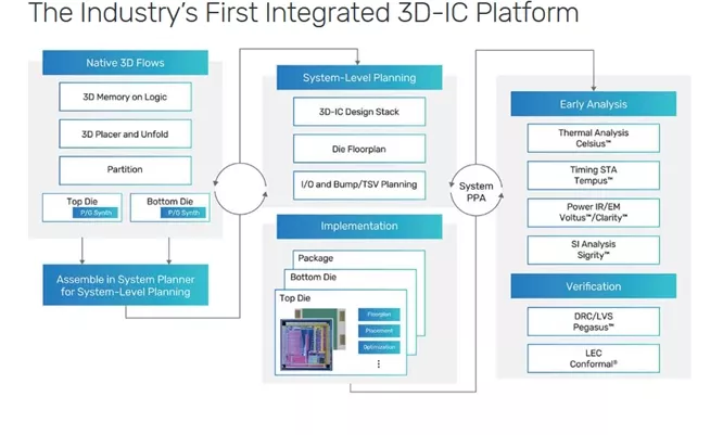
A single integrated environment helps teams evaluate architectural tradeoffs early, identify thermal or IR-drop risks, accelerate convergence, and reduce schedule uncertainty.
Frequently Asked Questions
When does 2.5D make a better choice than 3D-IC?
2.5D integration is ideal when the design has sufficient XY footprint, tighter thermal constraints, or a need to minimize manufacturing complexity and cost. It is also the preferred option when heterogeneous integration across multiple process nodes or foundries is required.
Can 2.5D meet AI bandwidth requirements?
Yes. The HBM-interposer architecture is the industry standard for GPUs and AI accelerators, delivering multi-terabit-per-second (TB/s) bandwidth.
Does 3D-IC replace 2.5D?
No. Both architectures will coexist. 2.5D dominates high-power compute today, and 3D-IC is rising in memory stacking and compact architecture.
Conclusion
As advanced packaging becomes the new path for semiconductor scaling, the choice between 2.5D and 3D-IC ultimately comes down to an architectural decision, balancing performance, density, thermals, manufacturability, and cost. Today, 2.5D remains the proven, high-yield choice for large AI and HPC designs. At the same time, 3D-IC is rapidly maturing into a critical technology for memory stacking, vertical logic-memory co-design, and compact compute modules.
Regardless of direction, success depends on a unified, system-level design approach and early cross-die analysis. Teams that evaluate thermal, electrical, and structural behavior upfront will significantly reduce schedule risk and achieve more predictable performance at tapeout.
Request a Design Assessment or Demo
If your team is exploring 3D-IC integration, you can request a design assessment to review stack feasibility, interposer requirements, and potential multiphysics risk areas. This collaborative evaluation helps identify where the Integrity 3D-IC Platform can improve integration efficiency, modeling accuracy, and time to signoff, giving your project a stronger foundation from the start.
- Explore the Cadence Multi-Die 3D-IC Solution to see how Cadence empowers next-generation system innovation.
- Explore the Integrity 3D-IC Platform to discover how 3D design and signoff enable system-level optimization.
- Talk to a 3D-IC Specialist to discuss your design challenges and roadmap.
Read More
Related Chiplet
- DPIQ Tx PICs
- IMDD Tx PICs
- Near-Packaged Optics (NPO) Chiplet Solution
- High Performance Droplet
- Interconnect Chiplet
Related Blogs
- What Is 3D-IC Technology? Fundamentals, Architecture, and Design Concepts
- 3D-IC Test and Reliability: KGD Strategies, Access Architecture, & Failure Mode
- Maximizing 3DIC Design Productivity with 3DBlox: A Look at TSMC’s Progress and Innovations in 2024
- Cadence Recognized for Accelerating AI and 3D-IC Applications by Samsung Foundry
Latest Blogs
- From horsepower to high-performance compute: automotive chiplets take the leap towards autonomous edge computing
- Designing the Future We Can Verify: A Vision for Multi-Die Design, STCO, and Trustworthy AI
- Wafer-Scale vs. Chiplets: The new war? - Part 2: Two Paths, One Wall
- Wafer-Scale vs. Chiplets: The new war?
- Chiplets 101: An Arteris Guide to Multi-Die Architecture