What Is 3D-IC Technology? Fundamentals, Architecture, and Design Concepts

As process nodes continue to advance into the sub-micron era, the limitations of traditional scaling are becoming increasingly evident. Larger monolithic chips are facing challenges such as higher power density, routing congestion, and reduced yield. Three-dimensional integrated circuits (3D-IC) technology represents a breakthrough approach by stacking multiple dies vertically. This design reduces communication paths, increases bandwidth, and significantly lowers energy consumption per bit. By bringing computation and memory closer together, 3D-ICs extend the trajectory of system-level performance, even as transistor scaling slows, marking a significant shift toward an era of vertical system integration.
Definition and Core Principles of 3D-ICs
A 3D integrated circuit (3D-IC) is a system composed of multiple active silicon dies stacked vertically and interconnected through fine-pitch vertical interconnects. Unlike traditional 2D integration, which spreads functionality across a single plane, 3D-IC technology bring logic, memory, and accelerators into tight physical proximity.
Core architectural principles include:
- Vertical Interconnects: Shorten communication paths, improving bandwidth and reducing energy per bit.
- Heterogeneous Integration: Combine dies from different process nodes or foundries to optimize performance and cost—for example, advanced logic with mature I/O or analog technologies.
- Chiplet Modularity: Partition large systems into smaller functional dies for improved yield and design flexibility.
- Improved Memory Locality: Vertically aligned compute and memory reduce latency and power overhead associated with off-chip data movement.
Together, these principles extend the industry’s ability to scale systems without relying exclusively on transistor miniaturization.
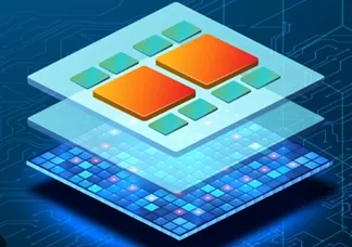
How Vertical Stacking and Chiplets Work Together
Two complementary approaches—vertical stacking and chiplet integration—enable 3D-IC architectures to achieve high performance, flexibility, and efficiency.
Vertical stacking takes integration further by physically aligning these dies in three dimensions. Memory or accelerators can be placed directly above compute tiles, dramatically reducing interconnect distances. The result is higher bandwidth, lower latency, and lower energy per bit—key benefits for data-intensive applications.
Examples of the :
- Compute units stacked beneath memory to reduce off-chip data transfer.
- Mixed-node integration combining high-speed logic with power-efficient analog and I/O technologies.
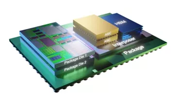
- High-bandwidth memory (HBM) stacked on GPUs and AI accelerators, where vertical data channels deliver massive bandwidth at lower power.
Together, chiplets and vertical stacking form the foundation of today’s scalable multi-die systems.
Key Building Blocks: TSVs, Interposers, and Hybrid Bonding
The integration of 3D-IC technology depends on a set of advanced interconnect and packaging technologies that define how dies communicate and share power.
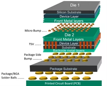
- Through-Silicon Vias (TSVs): Conductive vertical channels etched through silicon that enable low-latency, high-bandwidth inter-die signaling and power delivery.
- Interposers: Silicon substrates that connect multiple dies side-by-side (2.5D integration). They provide wide parallel data links and routing flexibility without requiring full stacking.
- Hybrid Bonding: Direct copper-to-copper die bonding that achieves ultra-fine-pitch vertical connections, ideal for logic-on-logic or memory-on-logic stacking.
Each of these technologies supports different density, performance, and cost goals. TSVs enable true 3D stacking, interposers facilitate chiplet assemblies, and hybrid bonding delivers the highest interconnect density available today.
Design Considerations: Floorplanning, Power, Timing, and Thermals
Transitioning from 2D to 3D design introduces a new level of complexity. The successful implementation of 3D-IC technology requires co-optimization across dies, packages, and systems, addressing challenges such as:
- Cross-Layer Floorplanning: Optimizing block placement across stacked dies to minimize routing length and manage thermal coupling.
- Power Delivery and Signal Integrity: Ensuring stable voltage supply through stacked structures using carefully co-designed TSV and interposer networks.
- Thermal Management: Managing heat concentration in stacked layers through thermal-aware placement, heat-spreading materials, and advanced cooling techniques.
- Timing and Synchronization: Modeling inter-die delay and skew precisely for accurate multi-die clock alignment.
These factors are crucial to achieving performance, reliability, and yield goals at the production scale.
Where 3D-ICs Fit vs Traditional SoC Approaches
As data-intensive workloads demand higher bandwidth and tighter memory coupling, 3D-IC technology offers a scalable solution.
Here’s how 3D-ICs compare:
- Memory Bandwidth: While monolithic SoCs rely on long external routing, stacked memory in 3D-ICs provides much wider, lower-energy bandwidth.
- Chiplet Integration: Large SoCs suffer yield penalties as die size grows. Modular chiplets in 3D-ICs reduce energy per bit and improve design flexibility.
- Design Scalability: Reticle stitching and high mask costs limit SoC scaling. Chiplet-based 3D designs enable reuse and faster iteration cycles.
By addressing these limitations, 3D-ICs enable power-efficient, high-performance systems ideally suited for AI, HPC, and networking applications.
Getting Started with 3D-IC Design Tools
Designing 3D-ICs requires integrated, system-driven workflows that unify die, package, thermal, and mechanical domains. Essential capabilities include:
- Multi-die stack visualization and planning
- Power and signal integrity analysis across dies
- Multiphysics thermal and mechanical modeling
- Unified implementation and verification environments
Cadence delivers a comprehensive toolset for this new era of system design:
- Integrity 3D-IC Platform: Enables die-level design, analysis, and inter-die connectivity with system-driven PPA optimization and seamless co-design across the 3D stack.
- Allegro X Advanced Package Designer Platform: Provides package-level optimization, interposer design, and advanced packaging configurations such as system-in-package (SiP) and fan-out wafer-level packaging (FOWLP).
Together, these platforms form the Cadence Multi-Die 3D-IC Solution, offering design teams a unified system view and the confidence to innovate without limits.
3D-IC – The Architectural Direction Going Forward
3D-IC technology marks a pivotal shift, from scaling in two dimensions to scaling in three. By bringing compute, memory, and accelerators closer together, 3D-ICs overcome data-movement bottlenecks and power inefficiencies that limit monolithic designs.
This modular, vertically integrated approach is shaping the future of computing, from AI and HPC to networking and edge devices, and defining how performance and efficiency will scale for decades to come.
Continue Exploring
To evaluate workflows and implementation strategies for multi-die and 3D-IC integration:
- Explore the Cadence Multi-Die 3D-IC Solution to see how Cadence empowers next-generation system innovation.
- Learn more about the Integrity 3D-IC Platform and Allegro X Advanced Package Designer Platform
- Talk to a 3D-IC expert to discuss your design challenges and roadmap.
Related Chiplet
- DPIQ Tx PICs
- IMDD Tx PICs
- Near-Packaged Optics (NPO) Chiplet Solution
- High Performance Droplet
- Interconnect Chiplet
Related Blogs
- What is a Chiplet, and Why Should You Care?
- How Cadence Is Expanding Innovation for 3D-IC Design
- What are Chiplets? - The Key Technology Behind Next-Gen Semiconductor Manufacturing
- 3D-IC Market Outlook: Technology Roadmaps, Readiness, and Design Implications
Latest Blogs
- Simulation Solutions for the Structural Integrity of Chip Packages
- Overcoming interconnect obstacles with co-packaged optics (CPO)
- Chiplets: 8 best practices for engineering multi-die designs
- Demystifying 3D ICs: A practical framework for heterogeneous integration
- Accelerating Next-Generation EMIB-T Packaging: A Collaboration Between Synopsys and Intel Foundry