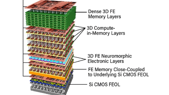
3D-IC Market Outlook: Technology Roadmaps, Readiness, and Design Implications By Reela Samuel December 22, 2025
Cadence 3D-IC Success Stories: Faster Bandwidth, Lower Power, On-Time Tapeouts By Reela Samuel December 22, 2025
3D-IC Test and Reliability: KGD Strategies, Access Architecture, & Failure Mode By Reela Samuel December 18, 2025
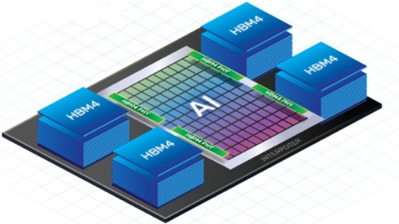
3D-IC in AI, HPC, and 5G: Bandwidth, Latency, and Energy per Bit Advantages By Reela Samuel December 16, 2025
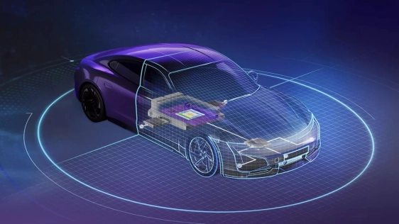
Bosch and the chiplet revolution: Enabling software-defined mobility By Michael Budde, President of Bosch Mobility Electronics December 15, 2025
Addressing the Biggest Bottleneck in the AI Semiconductor Ecosystem By Maksym Plakhotnyuk, CEO and Founder, ATLANT 3D December 15, 2025
Thermal Management in 3D-IC: Modeling Hotspots, Materials, & Cooling Strategies By Reela Samuel December 10, 2025
3D Chips: Socionext Achieves Two Successful Tape-Outs in Just Seven Months By Shekhar Kapoor December 9, 2025
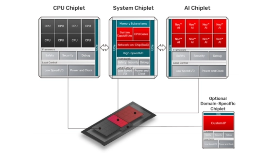
Intel Foundry Collaborates with Partners to Drive an Open Chiplet Marketplace By Chek-San Leong, Senior Director, Head of IP and Chiplet Ecosystem Alliance December 9, 2025
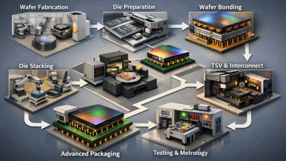
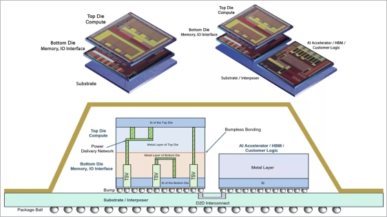
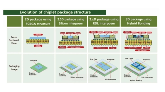
3D-IC Packaging: Wafer Stacking, Hybrid Bonding, and Interposer/RDL Techniques By Reela Samuel December 4, 2025
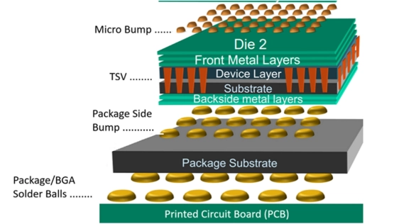
Through-Silicon Vias (TSVs): Interconnect Basics, Design Rules, and Performance By Reela Samuel December 2, 2025
The Semiconductor Back-End Process Explained: A Complete Picture of Product Packaging By Rapidus December 1, 2025
Light-speed ambition: GlobalFoundries acquires AMF and InfiniLink to power the AI datacenter revolution By Kevin Soukup November 27, 2025
The Growing Chiplet Ecosystem: Collaboration, Innovation, and the Next Wave of UCIe Adoption By UCIe™ Consortium November 26, 2025
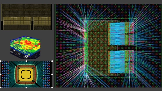
3D-IC Design Tools: Cadence Workflows for Planning, Assembly, and Analysis By Reela Samuel November 19, 2025
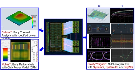
Signal integrity and power integrity analysis in 3D IC design By Todd Burkholder and John Caka November 18, 2025
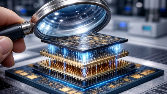
What Is 3D-IC Technology? Fundamentals, Architecture, and Design Concepts By Reela Samuel November 18, 2025
From Spec to Silicon: Successful Physical AI System Chiplet Bring-Up By Mick Posner November 13, 2025