3D-IC Design Tools: Cadence Workflows for Planning, Assembly, and Analysis

3D-IC design tools are becoming increasingly essential as the industry transitions toward chiplet architectures, heterogeneous integration, and advanced packaging to meet rising power, performance, and bandwidth demands. This blog introduces how Cadence addresses these challenges through the Integrity 3D-IC Platform, a unified workflow that connects planning, assembly, and multiphysics analysis into a single, coherent design environment.

In the earliest stages of development, engineering teams must assess stack architectures, bump and through-silicon via (TSV) budgets, interposer and redistribution layer (RDL) strategies, and system-level constraints, including thermal behavior, power delivery, and signal integrity (SI). These foundational considerations shape every subsequent phase of the 3D-IC design lifecycle and reinforce the need for a coordinated, data-consistent environment to achieve predictable design closure. When architectural planning, physical design, and multiphysics analysis operate in isolation, inconsistencies compound and impede integration, validation, and timing convergence.
The Unified 3D Stack Database and Cockpit
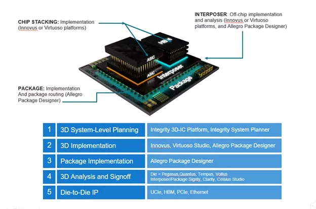
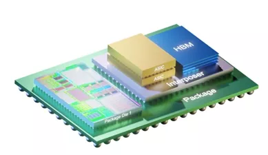
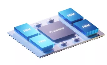
At the center of the Cadence Multi-Die 3D-IC Solution is a unified 3D stack database that serves as the single source for all stages of multi-die design. Instead of managing separate and often conflicting files for chiplets, bumps, redistribution layers, and package substrates, the Integrity 3D-IC Platform consolidates these elements into one fully synchronized system model. This comprehensive environment spans integration, advanced packaging, custom and digital implementation, verification, system analysis, and interconnect IP for chiplet-based designs.
This unified approach empowers engineering teams to visualize vertical stacking, lateral placement, and connectivity across every system partition. Designers can inspect placement hierarchies, verify physical alignment, and validate system connectivity in real time. Since the shared stack database directly feeds physical design and signoff engines, it eliminates version mismatches and data translation errors that traditionally slow down multi-die projects.
The cockpit interface enhances this workflow with interactive 2D and 3D visualization capabilities. System architects, chip designers, and packaging engineers can collaborate on the same structure simultaneously, creating a consistent foundation for exploration, physical planning, and final signoff.
Exploration and Stack Planning: Budgets for Bumps and TSVs
Early stack planning defines the system performance, thermals, and routing feasibility and performance of the entire 3D-IC architecture. With the Integrity 3D-IC Platform, architects can explore chiplet partitioning, bump arrays, and TSV configurations while applying constraints that capture bandwidth targets, signal integrity requirements, and physical alignment rules.
 The platform enables rapid experimentation with die ordering, die thickness, power delivery pathways, and interconnect density. Designers can develop bump budgets, estimate TSV counts, and assess architectural feasibility without the need for full physical implementation. This fast-feedback loop helps teams avoid configurations that may later result in routing congestion, thermal hotspots, or power delivery issues.
By modeling inter-die interfaces early, engineering teams can identify whether chiplets require additional I/O channels, a tighter micro-bump pitch, or revised die-to-die communication protocols. This early exploration improves system predictability and ensures that downstream implementation remains aligned with system-level goals.
Interposer and RDL Planning and Package Co-Design
Modern multi-die systems often rely on high-density interposer structures or advanced redistribution layers. These components must be designed in close coordination with chiplet placement and overall package layout to meet power integrity (PI), signal integrity, and cost objectives.
 The Integrity 3D-IC Platform integrates seamlessly with Cadence packaging solutions, enabling true co-design across chiplets, interposer routing, package layers, and substrate connectivity. The shared database allows packaging engineers to refine the interposer layout while chip teams validate I/O pad placement, net assignments, and physical constraints.
Stack planners can analyze routing channels, define power planes, and evaluate density constraints, while packaging engineers assess manufacturability and substrate cost. Because interposer and RDL models are connected to the same system-level database, electrical and physical alignment remain consistent throughout the design process.
This co-design approach minimizes rework, increases engineering efficiency, and accelerates system-level convergence.
Electro-Thermal, SI, PI, EM, and STA Signoff in One Loop
3D-ICs introduce new challenges in thermal behavior, power delivery, and high-speed signaling due to the proximity of vertically stacked dies. Addressing these challenges requires multiphysics analysis to be performed early and repeatedly throughout the design cycle. Cadence meets this need with a unified signoff loop that integrates thermal, electrical, timing, and electromigration analysis.
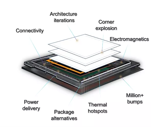
The Integrity 3D-IC Platform is directly linked to specialized Cadence solutions, including Celsius Thermal Solver for thermal analysis, Voltus IC Power Integrity Solution for power integrity (PI), Clarity 3D Solver for 3D electromagnetic (EM) extraction, and the Tempus Timing Solution for timing signoff. All analyses are performed on the same stack database used for implementation, eliminating manual handoffs, redundant data translation, or inconsistent geometry models.

When issues arise, such as thermal hotspots or power distribution network (PDN) resistance bottlenecks, designers can adjust placement, bump configurations, or power grid structures and rerun analysis rapidly. Because this loop is fully integrated, engineering teams gain early visibility into multiphysics risks and reduce costly, late-stage surprises.
Integrations and Data Exchange Across EDA Stages
3D-IC design is inherently multi-domain and requires tight integration across logic design, physical implementation, packaging, and verification. Cadence provides integrated data exchange paths that connect chip implementation tools, package design tools, and analysis engines, enabling seamless integration.
The Integrity 3D-IC Platform integrates directly with the Innovus Implementation System for die implementation, Allegro X Advanced Package Designer for substrate and interposer layout, and Virtuoso Studio for custom and analog design components. Connectivity and hierarchy are preserved end to end, and models transfer cleanly across domains without requiring extensive manual intervention.
The platform also supports open data exchange with partner companies and OSATs using standard industry formats. This reduces translation overhead, preserves design intent, and enables a smooth and reliable handoff throughout the ecosystem.
Sample Workflow: From Architecture to Signoff
A typical team using the Cadence Integrity 3D-IC Platform may follow this structured workflow:
- Architecture and partitioning: Evaluate chiplet candidates, explore stack ordering, and estimate TSV and bump budgets.
- System planning and co-design: Construct the unified 3D stack, model interposer or RDL structures, and align die I/O with package constraints.
- Implementation and connectivity validation: Transfer die-level data into implementation tools, validate inter-die connections, and refine placement.
- Multiphysics analysis loop: Run thermal, EM, SI, PI, and timing simulations and iterate accordingly to optimize system behavior.
- Assembly and integration: Ensure convergence between package and chip layouts and prepare system models for manufacturing review.
- Signoff: Leverage the integrated database for a comprehensive final signoff across timing, power, thermal, and reliability metrics.
This integrated workflow streamlines design cycles, minimizes integration risk, and enhances confidence in the final system's performance.
Request a Design Assessment or Demo
If your team is exploring 3D-IC integration, you can request a design assessment to review stack feasibility, interposer requirements, and potential multiphysics risk areas. This collaborative evaluation helps identify where the Integrity 3D-IC Platform can improve integration efficiency, modeling accuracy, and time to signoff, giving your project a stronger foundation from the start.
- Explore the Cadence Multi-Die 3D-IC Solution to see how Cadence empowers next-generation system innovation.
- Explore the Integrity 3D-IC Platform to discover how 3D design and signoff enable system-level optimization.
- Talk to a 3D-IC Specialist to discuss your design challenges and roadmap.
Read More:
Related Chiplet
- Interconnect Chiplet
- 12nm EURYTION RFK1 - UCIe SP based Ka-Ku Band Chiplet Transceiver
- Bridglets
- Automotive AI Accelerator
- Direct Chiplet Interface
Related Blogs
- Cadence Recognized for Accelerating AI and 3D-IC Applications by Samsung Foundry
- How Cadence Is Expanding Innovation for 3D-IC Design
- Navigating Chiplet-Based Automotive Electronics Design with Advanced Tools and Flows
- Thermal Analysis of 3D Stacking and BEOL Technologies
Latest Blogs
- Advancing Europe’s Automotive Chiplet Vision: Arteris Joins CHASSIS to Accelerate Software-Defined Mobility
- 3D-IC Market Outlook: Technology Roadmaps, Readiness, and Design Implications
- Cadence 3D-IC Success Stories: Faster Bandwidth, Lower Power, On-Time Tapeouts
- 3D-IC Test and Reliability: KGD Strategies, Access Architecture, & Failure Mode
- 3D-IC in AI, HPC, and 5G: Bandwidth, Latency, and Energy per Bit Advantages