Stop-For-Top IP model to replace One-Stop-Shop by 2025... and support the creation of successful Chiplet business
By Eric Esteve (PhD.) Analyst, Owner IPnest
The One-Stop-Shop model has allowed IP vendors of the 2000’s to create a successful IP business, mostly driven by consumer application, smartphone or Set-Top-Box. The industry has dramatically changed, and in 2020 is now driven by data-centric application (datacenter, AI, networking, HPC…), requiring best-inclass, high performance IP developed on bleeding edge technology nodes. That’s why the Stop-For-Top IP model should replace the One-Stop-Shop model during the 2020 decade and allow to supply the right IP more efficiently to the demanding customer involved in data-centric application. The next step will be to develop and market chiplet created from the Stop-For-Top IP portfolio, to help chip makers to overcome Moore’s law limitation and accelerate TTM for systems developed on technology nodes at 3nm and below. We think the IP vendors selecting Stop-For-Top IP model strategy will be the best positioned to offer chiplet at the right time when the semiconductor industry will need this innovation to overcome Moore’s law limitation.
During the 2010 decade the successful business model for Interface IP has been the One-Stop-Shop IP model. Offering to the IP customer a single place where he could buy several functions was a good way to help him taking the decision to buy, instead of to make, while minimizing admin and legal task. It was faster to negotiate and sign IP license contract with only one supplier than with many. But the nature of modern IP has changed, as they can’t be seen anymore as a commodity being cheaper to buy than to make. If we consider the star interface IP licensed for multi-million dollar, like PCIe 6 or CXL, DDR5 or HBM memory controller or PAM4 112G SerDes, designed on the most advanced technology node, performance, reliability, and robustness are now the essential pilar for decision making. We have shown that the Interface IP market has been extremely healthy on the 2016 to 2021, growing with 20% CAGR, passing from $520 million in 2016 to $1300 million in 2021. If we consider the 2021 to 2026 forecast of the interface IP category, there are clearly two groups of protocols. The first group include PCIe and CXL, DDR memory controller, Ethernet and SerDes and chip-to-chip protocols.
For these protocols, the largest part of IP revenues is generated by the most advanced functions targeting bleeding edge technology nodes. For the other protocols, the group of USB, MIPI, SATA or HDMI, both the weight and growth rate
are lower. It’s not a coincidence if in the last group, protocols are used in consumer type of applications like smartphone, PC or TV, or even automotive. Protocols from the first group are requested in applications like datacenter, HPC, networking, wireless base station, storage, etc. that we can summarize by enterprise.
Sounds like the old battle, consumer vs enterprise.
We have reworked the interface IP forecast for the next five years to extract the high-end part of PCIe and CXL, DDR memory controller, Ethernet and SerDes and chip-to-chip IP products, which are targeting advanced technology nodes, 7nm and below. The result can be synthetized on Table 1.
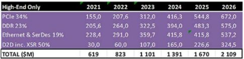
Picture 1: High-End Protocols Interface IP Forecast 2021-2026 Table
It can be interesting to compare these results with the total generated by all interface IP protocols for the same period:
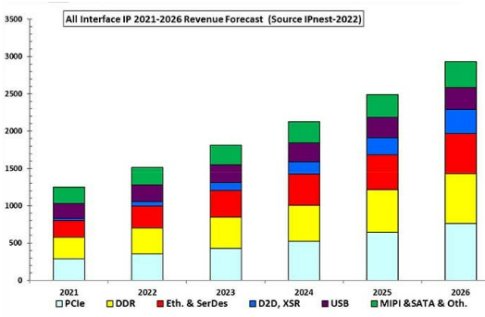
Picture 2: All Protocols Interface IP Forecast 2021-2026-Graphic

Picture 3: All Protocols Interface IP Forecast 2021-2026-Table
If in 2021 the high-end part of interface IP revenues are slightly less than 50% of the total, this part is constantly growing to reach 72% in 2026. The reason is linked with the five years CAGR, much larger for the group of high-end part:
- High-end PCIe and CXL CAGR 2021 to 2026 of 34%
- Advanced DDR Memory Controller CAGR 2021 to 2026 of 23%
- Ethernet and VHS SerDes CAGR 2021 to 2026 of 19%
- Chip-to-Chip including XSR CAGR 2021 to 2026 of 50%
- High-end above interface growing in average with CAGR 2021 to 2026 of 28%
When total interface protocol IP revenues are expected to grow with CAGR 2021 to 2026 of 19%.
For 2010 decade, two EDA vendors have successfully deployed One-Stop-Shop strategy, mostly targeting the interface protocol category, and have created a successful IP business. Synopsys has combined 55% market share (or $727 million) in 2021 in interface IP category by supporting every protocols. On top of PCIe and CXL, DDR memory controller, Ethernet and SerDes, Synopsys supports USB, MIPI, SATA, HDMI and Display Port. These added interconnect protocols are intensively used in consumer, industrial and automotive applications, but almost not selected in the “star” applications of the 2020 decade, the datacentric (datacenter, hyperscale, networking, HPC, AI, etc.).
The main question is to know if it will be possible to create a successful IP business during the 2020 decade by focusing only on the high-end data-centric interconnect protocols developed on advanced technology nodes, 7nm and below? If we consider the 2021 to 2026 forecast of high-end IP (Table 1), the segment which was looking like a niche market in 2020 is expected to become a two-billion-dollar market in 2026. The question becomes: would a vendor employing all engineering resources to support high-end data-centric interconnect protocols be able to reach 25% market share in 2026 and create a successful $500 million business?
An IP vendor able to position on Top IP only, by moving from well-known “One-Stop-Shop” model (selected by Synopsys and Cadence in the 2000’s) to “Stop-For-Top” model, will generate a better ROI. This IP vendor will differentiate from Synopsys and Cadence and extract higher IP revenues growth!
The goal is clear, the strategy will have to be defined and fine-tuned for each data-centric protocol, keeping in mind that the long-term process must be completed by the second step, market deployment of application specific chiplet, with specification based on the high-end data-centric IP portfolio. Stop-For-Top IP strategy is now clearly defined.
Step 1: Stop-For-Top IP strategy deployment by protocol
PAM4 SerDes 112G
The development of DSP based PAM4 SerDes is extremely complex and require building an excellent engineering team. Being the first to offer to the market a robust 112G SerDes, showing the best Bit Error Rate (BER) and demonstrating highest reliability is the key to engage a virtual cycle. New customer will select SerDes IP vendor based on market success, existing customers acting as reference for the quality of this very complex IP. PAM4 SerDes IP robustness is the killer argument in the selection process, even if latency, silicon area and power consumption should be optimized, but these parameters are ranked after robustness. Competitor 112G SerDes demonstrating much lower power consumption (or area, or latency) but being unstable once implemented will never make the decision.
Because PCIe and CXL PHY are derived from SerDes, demonstrating well designed SerDes will greatly help offering best in class PCIe/CXL PHY.
PCIe and CXL IP solution
PCIe is used in many applications ranging from test equipment to automotive, including enterprise. Datacentric, AI and HPC are clearly the first adopter for the latest PCIe standard release. That’s why we consider PCIe 5 and 6 to be the flagship offer for Stop-For-Top IP. Demonstrating compliance with the standard of the PCIe IP solution and interoperability is a must-have for this protocol and the controller must be designed supporting all the features defined in the specification. This will allow to provide the best possible support to extremely demanding customers. Such a positioning will require that verification has been exercised on customer precise selection, as the possible configurations are very high due to the numerous features. Stop-For-Top PCIe IP associate a very reliable PHY (offering excellent BER) and a features-rich controller, the solution being fully verified and interoperable.
CXL solution can be derived from the PCIe IP, but the PHY and the controller have been optimized for best possible latency while keeping excellent BER. At this stage, PCIe 6 and CXL are selected by early adopter to be integrated into chips targeting advanced technology node (5nm) developed with an aggressive schedule.
The guarantee to select a stable, robust IP solution is by far the most important care about for early adopter. That’s why offering optimized PPA (area and power consumption) will come later, for a second-generation IP.
DDR Memory Controller (LPDDR5/4, HBM 2/2E)
DDR memory controller IP has been the pilar of external sourcing of IP for SoC design. If this function doesn’t work properly, the SoC can’t be released to production (unlike with USB or HDMI IP, for example). This specificity helps to define the quality requirement associated with this IP perfection must be the rule.
The high bandwidth requirement of data-centric application is pushing to use the latest release of memory controller showing highest data-rate (LPDDR5) or High Bandwidth Memory protocol (HBM2E).
D2D interconnect (XSR and UCIe)
Extra Short Reach (XSR) D2D standard allows serially interconnecting two chips using one or more SerDes which can run up to 112 Gbps on ultra short distance. The other option is to use parallel-based data transfer with forwarded clock operating in the 4 GT/s to 32 GT/s range (see Picture 4) in the Universal Chiplet
Interconnect Express, or UCIe. UCIe formally announced in March 2022 is emerging as a standard protocol, counting almost 40 contributor members and may solve the issue created by the multiplication of D2D protocols, including in-house. According with Intel “Integrating multiple chiplets in a package to deliver product innovation across market segments is the future of the semiconductor industry and a pillar of Intel’s IDM 2.0 strategy. Critical to this future is an open chiplet ecosystem with key industry partners working together under the UCIe Consortium toward a common goal of transforming the way the industry delivers new products and continues to deliver on the promise of Moore’s Law.”
The parallel, clock forwarded UCIe protocol, offer a strong advantage to enable a much lower latency and lower power consumption, compared to XSR SerDes. We expect UCIe to greatly help to create an open chiplet ecosystem.
To fulfill the need for ever increasing bandwidth has put pressure to move faster to target bleeding edge technology nodes and to release faster new version of interconnect protocols (PCIe, Ethernet, memory controller). Innovation like PAM4 modulation and creation of DSP-based SerDes to replace old, 100% analogbased
technique, were implemented, allowing to break the 100Gbps barrier. Innovative architecture has been defined pushing adoption of new standard like CXL, supporting cache-coherent memory sharing for processor, co-processor and AI accelerator, or Chip-to-Chip protocol between main SoC and chiplet, allowing to pass the technological area limit and offer more powerful system in a single package to support ever increasing needs to compute and interconnect data flow, like in the year 2000 using a SoC has led to smartphone explosion.
If we synthetize, the next technology revolution will require using top interconnect and IP vendors will have to propose best-in-class interface IP, like above described, to create a successful IP business based on Stop-For-Top IP positioning. We think that offering Stop-For-Top IP should be the first step of a strategy, the final goal being to offer a chiplet portfolio, built by integrating already available interconnect IP into an Integrated Chip (IC), commonly named chiplet. To support this strategy, IP vendor will have to rely on a pool of dedicated resources specialized in ASIC design service. IP vendor will have to build this engineering team, whether organic or inorganic, by acquisition of an ASIC design service vendor.
Step 2: chiplet portfolio derived from Stop-For-Top IP
There is now consensus in the industry that a maniacal focus on achieving Moore’s law is not valid anymore for advanced technology nodes, eg. 7nm and below. Chip integration is still happening, with more transistors being added per sq. mm at every new technology node. However, the cost per transistor is growing higher
every new node as well. Chiplet technology is a key initiative to drive increased integration for the main SoC while using older nodes for other functionality. This hybrid strategy decreases both the cost and the design risk associated with integration of other Design IP directly onto the main SoC.
Integration of a central SoC plus various accelerator or I/O chiplet in the same package is seen as the solution to overcome the challenge facing Moore’s law. This strategy is effective for scaling not only server CPUs, but also for heterogeneous design of complex systems. Heterogeneous chiplet design allows us to target different applications or market segments by modifying or adding just the relevant chiplet while keeping the rest of the system unchanged. New developments could be launched quicker to the market, with significantly lower investment, as redesign will only impact the package substrate used to house the chiplet.
In fact, IP vendors have the best know-how to implement on silicon a function that they have designed to be a Stop-For-Top IP. For complex Design IP, even if simulation verification has been run before shipping to customers, vendors must validate the IP on silicon to guarantee performance. For digital IP, the function
can be implemented in FPGA because it’s faster and far less expensive than making a test chip. For mixessignal IP, like a SerDes based PHY, vendors select the Test Chip (TC) option enabling to run characterization of the IP in silicon before shipping to customer. Even though a chiplet is not simply a TC, because it will be
extensively tested and qualified before being used in the field, the amount of incremental work to be done by the vendor to develop a production chiplet is far less.
In other words, the IP vendor is the best positioned to quickly release a chiplet built from his own IP, offer the best possible TTM and minimize risk. The business model for heterogeneous integration is in favor of various chiplet being made by the relevant IP vendor since he is owner of the Design IP and has the knowhow
to properly integrate the function with the best TTM. In fact, IP vendors have the best know-how to implement on silicon a function that they have designed to be a Stop-For-Top IP. Nevertheless, chip makers can design their own chiplet, implementing house-made interconnects to protect their unique architecture,
or source already available Stop-For-Top IP, if the development schedule allow to better comply with aggressive TTM requirements.
Unfortunately, the various protocol standards are not synchronized by a single organization. New PCIe standard can come one year (or more) earlier or later than the new Ethernet protocol standard. Using heterogeneous integration allows silicon providers to adapt to the fast-changing market by changing the design of the relevant chiplet only. Adopting this strategy provides better TTM and minimizes design cost for a new product, while better targeting end markets, compared to a general SoC. Considering that advanced SoC design fabrication requires massive capital expenditures for 5nm, 3nm or even more advanced process nodes, the impact of chiplet architectures will be tremendous to drive future innovation in the semiconductor space.
Chip maker developing SoCs for high-end applications, such as HPC, datacenter, AI or networking are likely to be early adopters for chiplet architectures. Specific functions, like AI accelerators, Ethernet, PCIe or CXL standards should be the first interface candidate for chiplet designs. When these early adopters have
demonstrated the validity of heterogeneous chiplet architecture, leveraging multiple different business models, and obviously the manufacturing feasibility for test and, packaging, it will create an ecosystem that is critical to support this new technology. At this point, we can expect a wider market adoption, not only for high-performance applications.
Like it was the case for Design IP sourcing to build a SoC in the 2000’s, the buy or make decision for chiplet sourcing to complete a system design, will be weighted between core competency protection and sourcing of non-differentiating functions. The historical and modern-day Design IP business growth since the 2000’s has been sustained by continuous increase of external sourcing. Both models will coexist (chiplet designed in-house or by a vendor) but history has shown that the buy decision eventually overtakes the make.
IPnest believes this trend will have two main effects in the interface IP business, one will be the strong growth of D2D IP revenues on the short term (2021-2025), and the other is the creation of the heterogenous chiplet market issued from Stop-For-Top IP portfolio. This market is expected to consist of complex protocols
functions like PCIe, CXL or Ethernet. Even IP vendors delivering USB, HDMI, DP, MIPI interface IP integrated in SoCs I/O may decide to deliver I/O chiplet instead.
If Stop-For-Top Interface IP vendors may be major actors in this silicon revolution, the silicon foundries addressing the most advanced nodes like TSMC and Samsung will also play a key role. We don’t think foundries will design chiplet, but they could make the decision to support IP vendors and push them to design chiplet to be used with SoCs in 3nm, like they do today when supporting advanced IP vendors to market their high-end SerDes as hard IP in 7nm and 5nm. IPnest has identified a few IP vendors in position to select this two-step strategy and market chiplet now or in the future, like Alphawave IP, Rambus or Credo Semiconductor.
Intel’s recent transition to 3rd party foundries is expected to also leverage third party IPs, thanks to UCIe consortium allowing to create an open chiplet ecosystem sustained by heterogenous chiplet adoption by semiconductor heavyweights. In this case, no doubt that Hyperscalars like Microsoft, Amazon, Meta or Google will also adopt chiplet architectures…
The Stop-For-Top IP model is the first step of a successful strategy followed by the creation of a chiplet portfolio by IP vendors to support industry need for open chiplet ecosystem. This ecosystem is needed by the semiconductor industry to overcome Moore’s Law limitation and reach the trillion dollars during the 2020 decade.
By Eric Esteve (PhD.) Analyst, Owner IPnest
About the Author: Eric Esteve (PhD.) has been part of the DAC IP committee between 2016 and 2020, has posted more than 400 blogs in Semiwiki, articles, white papers or success stories since 2011. He has worked as ASIC designer (1983-1992) then in various sales & marketing positions with TI, Atmel, PLDA and Snowbush (1992-2008), before creating IPnest in 2008. IPnest market the “Interface IP Survey” and the “Design IP Report”, covering the overall IP market by category (CPU, GPU, DSP, Interface, Mixed-signal, etc.). IPnest’s customer list counts major foundries, IP vendors and IDM or Fabless, totalizing more than 45 satisfied customers. IPnest is simply considered as the best Design IP analyst
on a world-wide basis.
This white paper has been sponsored by Alphawave IP, nevertheless the content reflects the author’s positioning about the IP market and the way it expected to evolve in the future, during the 2020 decade.
Related Chiplet
- DPIQ Tx PICs
- IMDD Tx PICs
- Near-Packaged Optics (NPO) Chiplet Solution
- High Performance Droplet
- Interconnect Chiplet
Related Technical Papers
- 3DIO IP For Multi-Die Integration
- IP for 3D Multi-Die Designs
- REX: A Remote Execution Model for Continuos Scalability in Multi-Chiplet-Module GPUs
- LaMoSys3.5D: Enabling 3.5D-IC-Based Large Language Model Inference Serving Systems via Hardware/Software Co-Design
Latest Technical Papers
- WarPGNN: A Parametric Thermal Warpage Analysis Framework with Physics-aware Graph Neural Network
- DUET: Disaggregated Hybrid Mamba-Transformer LLMs with Prefill and Decode-Specific Packages
- DS2SC-Agent: A Multi-Agent Automated Pipeline for Rapid Chiplet Model Generation
- In-SoIC ESD Protection for Chiplet-Based 3D Microsystems: Future Research Directions
- ODIN-Based CPU-GPU Architecture with Replay-Driven Simulation and Emulation