Achieving Better Chiplet Design Signal Integrity with UCIe™
By Tim Wang-Lee, Ph.D. Signal Integrity Application Scientist at Keysight Technologies
Chiplet design marks a transformative shift in the semiconductor industry, delivering improved performance, cost efficiency, and scalability. Yet, this innovative approach brings unique signal integrity (SI) challenges that require standards for reliable operation and future compatibility. This blog covers:
- Understanding the Signal integrity (SI) challenge in chiplet designs
- Evaluating your SI with Universal Chiplet Interconnect Express™ (UCIe™) standard
- Exercising the best practices for improving your SI
Signal Integrity Challenges in Chiplet Designs
Despite its benefits, the chiplet design approach presents unique challenges. Unlike conventional large-monolithic-die designs, chiplet-based designs segment various functions into smaller, individual dies. This approach enhances cost efficiency, yield, and scalability. However, this introduces:
- Increased system design complexity
- Challenges in chiplet die-to-die (D2D) communication
As a result, robust signal integrity of the D2D communication is crucial in establishing the reliability and interoperability of chiplet-based designs. Key components of D2D signal integrity (SI) include:
Loss
The frequency-dependent loss from D2D interconnects attenuates high-frequency components more than lower-frequency ones, causing rise time degradation. This low-pass behavior alters the frequency spectrum of the input data, see Figure 1.
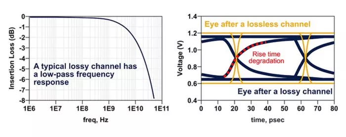
Figure 1. Left: A typical interconnect has a low-pass frequency response. Right: The low-pass frequency response causes rise time degradation. The degradation manifests in the edge transition of the eye diagram, indicated by the red dotted line.
Crosstalk
As interconnect density increases and traces are placed closer to each other, crosstalk becomes a significant concern. Energy from adjacent interconnects can couple to transmitted data line, introducing noise that degrades signal integrity. Figure 2 shows the impact of far-end crosstalk on the received eye.
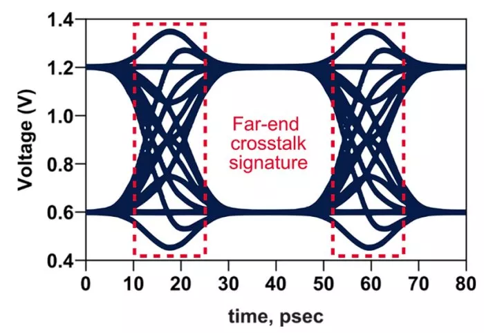
Figure 2. The energy of close-by signal lines (aggressors) can couple into the data line of interest (victim), causing peaking in the transition area of the eye diagram, indicated by red dotted rectangles.
UCIe Standard’s Guidance for Chiplet SI Analysis
The UCIe standard provides electrical layer specifications to ensure robust SI in interconnects. Key features include:
VTF Loss
The voltage transfer function (VTF) loss metric helps determine if an interconnect is too lossy. To pass, the VTF loss line must be above the UCIe VTF loss mask. Plotting your data line's VTF loss line against the VTF loss mask can help you quickly evaluate your design's performance.
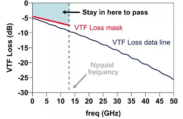
Figure 3. The UCIe standard provides VTF loss metrics for different data rates and packaging types. To pass the VTF loss metric, the VTF loss curve has to stay above the VTF loss mask specified for the given data rate and packaging type.
VTF Crosstalk
VTF crosstalk is defined as the power sum of the ratios of the aggressor receiver voltage to the source voltage [1]. This helps in assessing the impact of crosstalk on signal integrity. The plot below demonstrates a data line that fails the VTF crosstalk metric.
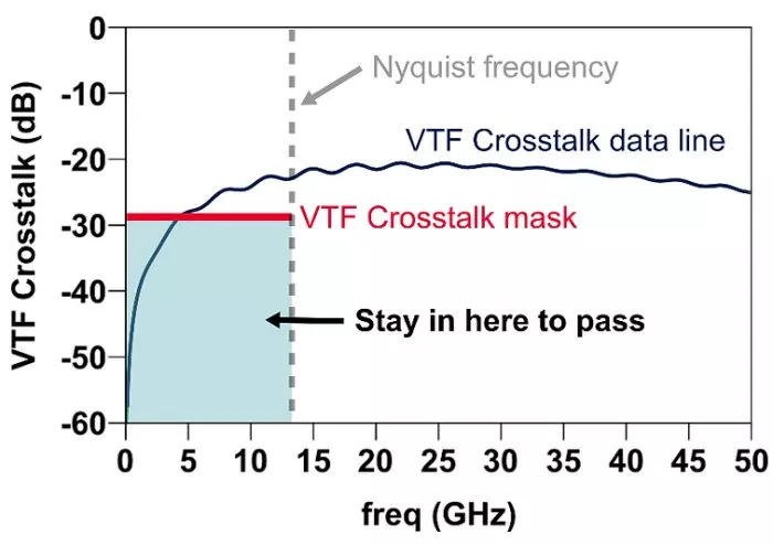
Figure 4. The UCIe standard provides VTF crosstalk metrics for different data rates and packaging types. To pass the VTF crosstalk metric, the VTF crosstalk curve has to stay below the VTF crosstalk mask specified for the given data rate and packaging type.
Eye Mask and Equalization
The UCIe standard specifies eye masks for different data transfer rates, ensuring the signal quality meets the required thresholds. Based on data rates, equalization on the transmitter (Tx) and receiver (Rx) is recommended or required. Figure 5 shows an example of the application of Tx de-emphasis and the UCIe eye mask.
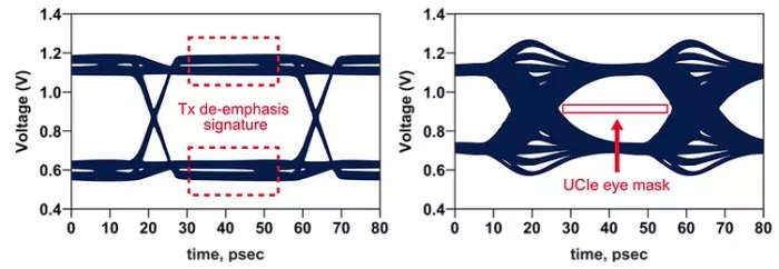
Figure 5. Left: An example of the transmitter eye diagram when the transmitter includes de-emphasis. Right: The UCIe standard provides eye masks to evaluate the performance of a given link. Proper Tx and Rx equalization can improve the eye-opening.
Improve the SI of Your Chiplet Designs
My Ph.D. advisor always says, “The best way to solve any signal integrity problem is to find the root cause.”
To address excessive loss and VTF loss mask violations, start by examining the length of the traces. To reduce crosstalk, increase the spacing between the traces. Transmitter and receiver equalization should be a last resort to improve your SI. Remember to use Electronic Design Automation software to help you enforce the UCIe metrics while you analyze the SI of your chiplet interconnects.
Addressing the root causes of SI issues can enhance signal integrity and help you understand the limitations of your current design.
Conclusion
Signal integrity is critical for successful chiplet designs. The UCIe standard provides comprehensive guidelines to address SI challenges, ensuring reliable and high-performance chiplet-based solutions. For more detailed information and resources, visit the UCIe website.
References
-
"Universal Chiplet Interconnect Express (UCIe) Specification," July 10, 2023, Revision 1.1, Version 1.0.
Related Chiplet
- DPIQ Tx PICs
- IMDD Tx PICs
- Near-Packaged Optics (NPO) Chiplet Solution
- High Performance Droplet
- Interconnect Chiplet
Related Technical Papers
- Signal Integrity Challenges in Chiplet-Based Designs: Addressing Performance and Security
- Advanced Chiplet Placement and Routing Optimization considering Signal Integrity
- Tiny Chiplets Enabled by Packaging Scaling: Opportunities in ESD Protection and Signal Integrity
- RapidChiplet: A Toolchain for Rapid Design Space Exploration of Chiplet Architectures
Latest Technical Papers
- Expert Streaming: Accelerating Low-Batch MoE Inference via Multi-chiplet Architecture and Dynamic Expert Trajectory Scheduling
- WarPGNN: A Parametric Thermal Warpage Analysis Framework with Physics-aware Graph Neural Network
- DUET: Disaggregated Hybrid Mamba-Transformer LLMs with Prefill and Decode-Specific Packages
- DS2SC-Agent: A Multi-Agent Automated Pipeline for Rapid Chiplet Model Generation
- In-SoIC ESD Protection for Chiplet-Based 3D Microsystems: Future Research Directions