Advanced Chiplet Placement and Routing Optimization considering Signal Integrity
By Haeyeon Kim, Junghyun Lee, Seonguk Choi, Federico Berto, Taein Shin, Joonsang Park, Jihun Kim, Jiwon Yoon, Byeongmok Kim, Youngwoo Kim, and Joungho Kim
Abstract:
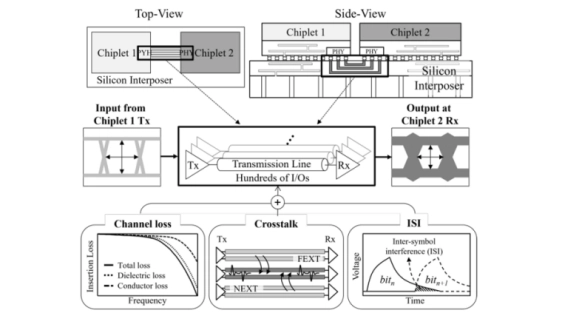
This article addresses the critical challenges of chiplet placement and routing optimization in the era of advanced packaging and heterogeneous integration. We present a novel approach that formulates the problem as a signal integrity-aware hierarchical Markov decision process (MDP), leveraging the place-to-route (P2R) algorithm. Our method uniquely incorporates the universal chiplet interconnect express (UCIe) eye mask specifications to ensure compliance with datarate-dependent signal integrity requirements. Tested on 10 benchmark problems, P2R achieved superior results with an average eye-diagram aperture of 0.869 unit interval (UI) in a single iteration, outperforming random search and deep reinforcement learning by 44.8%. By addressing the combinatorial complexity and hard constraints inherent in chiplet-based designs, this approach enables optimization while ensuring compliance with industry standards. Our work represents a significant advancement in optimizing heterogeneous integrated systems, addressing challenges that conventional placement and routing methods cannot adequately solve.
To read the full article, click here
Related Chiplet
- DPIQ Tx PICs
- IMDD Tx PICs
- Near-Packaged Optics (NPO) Chiplet Solution
- High Performance Droplet
- Interconnect Chiplet
Related Technical Papers
- Signal Integrity Challenges in Chiplet-Based Designs: Addressing Performance and Security
- Tiny Chiplets Enabled by Packaging Scaling: Opportunities in ESD Protection and Signal Integrity
- Intel Delivers Cutting-Edge Process Technologies to the Data Center with Intel 18A and Advanced Chiplet Packaging
- Achieving Better Chiplet Design Signal Integrity with UCIe™
Latest Technical Papers
- Link Quality Aware Pathfinding for Chiplet Interconnects
- Effects of Poor Workload Partitioning on System Performance for Chiplet-Based Systems
- Mozart: Modularized and Efficient MoE Training on 3.5D Wafer-Scale Chiplet Architectures
- Network Design for Wafer-Scale Systems with Wafer-on-Wafer Hybrid Bonding
- CarbonPATH: Carbon-aware pathfinding and architecture optimization for chiplet-based AI systems