Chiplet-Based Techniques for Scalable and Memory-Aware Multi-Scalar Multiplication
Florian Hirner, Florian Krieger, Sujoy Sinha Roy
Graz University of Technology, Austria
Abstract
This paper presents a high-performance architecture for accelerating Multi-Scalar Multiplication (MSM) on ASIC platforms, targeting cryptographic applications with high throughput demands. Unlike prior MSM accelerators that focus solely on efficient processing elements (PEs), our chiplet-based design optimally balances area, power, and computational throughput. We identify a mixed window configuration of 12- and 13-bit windows that enables an efficient multi-PE integration of 10 PEs per chiplet. Our single-PE design achieves a 1.37x speedup and 1.3x area reduction over prior works, while the multi-PE chiplet design improves the area-time product by 2.2x, offering scalability, lower production costs, and higher manufacturing yields.
Index Terms—Multi-Scalar Multiplication, Zero-knowledge proofs, Hardware Acceleration, Scalable Chiplet Architecture, Parallel Computing
I. INTRODUCTION
Multi-Scalar Multiplication (MSM) is a computationally intensive operation in cryptographic protocols, particularly in pairing-based zero-knowledge proofs (ZKPs) [1]. As shown in Figure 1, MSM accounts for over 70% of proof generation time [2]. Its computational dominance increases with the number of points N, as seen in systems like Groth16 [3], PlonK-KZG [4], and Marlin-KZG [5], which process tens to hundreds of gigabytes of data and take minutes for 225 to 228 points. Hardware acceleration of MSM is crucial for improving the time and energy of proof generation.
CycloneMSM [6] and Hardcaml [7] are high-performance FPGA-based MSM accelerators from the 2023 Z-Prize [8] challenge. These designs leverage Pippenger’s bucket method [9] to accelerate MSM by decomposing [10] it into three key steps: bucket classification, bucket aggregation, and result aggregation. The two accelerators optimize the computationally dominant bucket classification step and use a single fully pipelined point adder unit. However, due to the large size of fully pipelined point adder, these accelerators cannot instantiate more than one processing element (PE) even in high-end FPGAs. ASIC architectures such as PipeZK [11], Gypsophila [12], and PriorMSM [13] primarily employ single processing element (PE) configurations with optimized memory access strategies to mitigate bandwidth pressure from bucket collisions during classification. Among these, only Gypsophila [12] explores a multi-PE design where each PE independently computes separate MSMs.
Notably, no prior work has investigated a collaborative multi-PE MSM design where all PEs work together on a single MSM computation. Such a design could significantly reduce latency and enhance throughput.
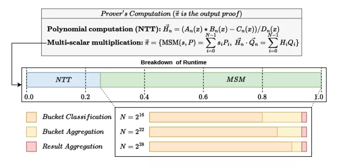
Fig. 1. Overview of workload distribution for NTT, MSM, and Bucketing operations involved in proof generation of paring-based ZKPs.
Motivation for chiplet-based MSM design approach:
Instantiating multiple PEs for MSM increases the overall area of the ASIC design, which can escalate production costs and negatively impact yield due to the complexities associated with fabricating large chips. For example, as shown in Table I, a monolithic ASIC accelerator with 16-bit window size and 16 PEs would require approximately 269mm2 of die area which is large. In modern semiconductor engineering, multi-chiplet System-in-Package (SiP) provides an effective solution to address cost and yield challenges of large monolithic chips. Decomposing the design into smaller and modular chiplets not only improves scalability and manufacturing yield but also reduces production costs [14]. Recent works – such as CiFHer [15], REED [16] and Chiplever [17] – have ex-plored the adoption of chiplet-based architectures for Fully Homomorphic Encryption (FHE), which like MSM is also computation and data intensive. This motivates us to explore the research question: How can MSM be implemented as a multi-chiplet SiP to achieve high performance?
Our contributions are summarized as follows:
- Memory aware PE Design: We analyze the impact of memory footprint and latency on PEs and propose an optimized design that balances area and computational throughput for MSM workloads.
- Mixed window sizes: We introduce mixed window size configurations for multi-PE setups, demonstrating how they optimize memory usage and workload distribution while minimizing latency.
- Inter-chiplet communication: We propose diverse work-load distribution and interconnect strategies that minimize inter-chiplet and off-chip memory communications. We use these distribution strategies (vertical, horizontal or full unrolling) to propose three different chiplet-based architectures.
- Comprehensive evaluation: We evaluate our design across varying configurations, showing up to 1.14× and 2.2× improvements in throughput and area efficiency, respectively, compared to state-of-the-art monolithic de-signs. In addition, our chiplet-based design enhances the scalability and production yield for ASIC platforms.
To read the full article, click here
Related Chiplet
- DPIQ Tx PICs
- IMDD Tx PICs
- Near-Packaged Optics (NPO) Chiplet Solution
- High Performance Droplet
- Interconnect Chiplet
Related Technical Papers
- ChipAI: A scalable chiplet-based accelerator for efficient DNN inference using silicon photonics
- FoldedHexaTorus: An Inter-Chiplet Interconnect Topology for Chiplet-based Systems using Organic and Glass Substrates
- AuthenTree: A Scalable MPC-Based Distributed Trust Architecture for Chiplet-based Heterogeneous Systems
- A physics-constrained and data-driven approach for thermal field inversion in chiplet-based packaging
Latest Technical Papers
- Escaping Flatland: A Placement Flow for Enabling 3D FPGAs
- 3D optoelectronics and co-packaged optics: when solving the wrong problems stalls deployment
- Expert Streaming: Accelerating Low-Batch MoE Inference via Multi-chiplet Architecture and Dynamic Expert Trajectory Scheduling
- WarPGNN: A Parametric Thermal Warpage Analysis Framework with Physics-aware Graph Neural Network
- DUET: Disaggregated Hybrid Mamba-Transformer LLMs with Prefill and Decode-Specific Packages