Are Chiplets Enough to Save Moore's Law?
By Steve Leibson, EETimes (June 2, 2023)
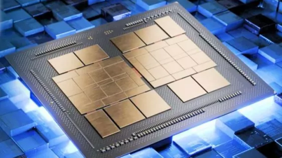
During a press conference at Computex this week in Taiwan, Nvidia CEO Jensen Huang and MediaTek CEO Rick Tsai announced that Nvidia would be supplying GPU chiplets to MediaTek to be incorporated into a yet-to-be-designed system-on-chip (SoC) for in-cabin automotive applications along with Nvidia AI and graphics IP.
Chiplets are not new to Nvidia. This announcement also adds a bit more validation for chiplets as a concept—one that many semiconductor makers are counting on to help keep Moore’s Law alive for the next several years.
The idea behind chiplets is hardly a new concept. The industry has been making multi-chip modules for decades: Mostek, for example, put two MK4116 16-Kbit DRAM chips in a dual-cavity ceramic package to create the MK4332D 32Kbit DRAM back in 1979. Intel also mated a CPU chip and an SRAM chip in the Pentium Pro, introduced in late 1995. These multichip modules (MCMs) allowed Mostek and Intel to transcend the limitations of their semiconductor processes to create packaged devices that were “more than Moore.
To read the full article, click here
Related Chiplet
- DPIQ Tx PICs
- IMDD Tx PICs
- Near-Packaged Optics (NPO) Chiplet Solution
- High Performance Droplet
- Interconnect Chiplet
Related News
- Imec’s Van den hove: Moving to Chiplets to Extend Moore’s Law
- Is Chiplets the Answer to the End of Moore’s Law?
- The keeper of Moore’s Law
- Faraday Unveils 2.5D/3D Advanced Package Service for Chiplets
Latest News
- Adeia Enters into Multi-Year IP License Agreement with AMD
- STMicroelectronics enters high-volume production of its industry-leading silicon photonics platform to support AI infrastructure demand
- Vertical Compute raises €57M to solve the AI memory bottleneck with new high density memory
- Ayar Labs Closes $500M Series E, Accelerates Volume Production of Co-Packaged Optics
- NanoIC opens access to first-ever fine-pitch RDL and D2W hybrid bonding interconnect PDKs