OKI Develops Tiling crystal film bonding (CFB) Technology for Heterogeneous Integration of Optical Semiconductors onto 300 mm Silicon Wafers
Contributing to the advancement of photonics-electronics convergence technology and working with partners for early commercialization
TOKYO, August 14, 2025 -- OKI (TOKYO: 6703) has successfully developed Tiling crystal film bonding (CFB)1 technology using its proprietary CFB technology. This technology makes possible the heterogeneous integration of small-diameter optical semiconductor wafers onto 300 mm silicon wafers, heretofore not possible due to wafer size restrictions, and will contribute to the advancement of rapidly growing photonics-electronics convergence technology 2. OKI aims to achieve early commercialization through collaboration with partner companies and universities.
Rapid advances in artificial intelligence (AI) in recent years has fueled growing demand for data centers, making it a serious social issue to suppress increases in power consumption while expanding data processing capabilities. One solution to such a challenge currently drawing attention is technologies that achieve high-density, high-speed transmission, and low power consumption, applying photonics-electronics convergence technology that combines electronic and optical circuits. In particular, the heterogeneous integration of optical semiconductors onto silicon wafers is expected to improve performance still further by enabling the integration of silicon photonics 3 with optical semiconductors.
Nevertheless, heterogeneous integration presents various technical challenges. For example, while silicon photonics use large-diameter 200 mm (8-inch) or 300 mm (12-inch) silicon wafers, optical semiconductor wafers such as InP (indium phosphide) wafers are typically smaller 50 mm (2-inch) to 100 mm (4-inch) compound semiconductor wafers due to the difficulty of achieving epitaxial growth. Additionally, silicon optical waveguides require nanoscale roughness control, which in turn requires heterogeneous integration processes that avoid causing damage.
Overview of Tiling CFB technology
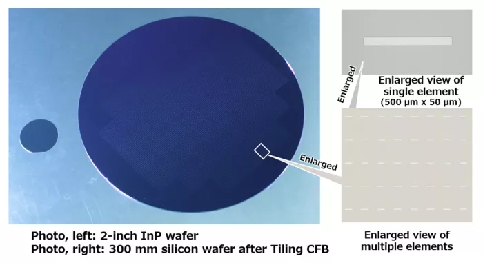
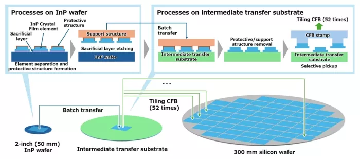
The Tiling CFB technology developed by OKI overcomes this disparity in wafer sizes and allows heterogeneous integration without causing damage. The technology allows for 52 repeated tiling operations over the entire surface of a 300 mm silicon wafer using a single 2-inch InP wafer, enabling efficient use of InP-based materials. The InP wafer can be reused as is after transfer to allow material recycling and reuse, helping reduce the environmental burden. Placement accuracy is approximately ±1 µm, with an angular accuracy of ±0.005°. This high accuracy, when combined with OKI's proprietary 3D intersecting waveguide 4 silicon photonics technology, realizes high-efficiency optical coupling between optical semiconductors and silicon waveguides.
In a demonstration, a sacrificial layer and InP-based Crystal Films functioning as optical semiconductors were epitaxially grown on a 2-inch InP wafer, then separated into individual elements. A protective structure to prevent chemical attack when etching the sacrificial layer and a support structure for batch transfer were formed on each element. This enabled the InP-based Crystal Films to be successfully batch-transferred to an intermediate transfer substrate without erosion. Batch transfer to an intermediate transfer substrate is carried out to protect the silicon wafer from damage during the subsequent removal process, as removing the protective structure and support structure on the intermediate transfer substrate prevents damage to the silicon wafer during the removal process. The unique design of the intermediate transfer substrate ensures that the InP-based Crystal Films do not peel off, maintain adhesion during the process of removing the protective structure and support structure, and are easily transferred during the transfer process.
Furthermore, by repeatedly transferring Crystal Films from the intermediate transfer substrate using a CFB stamp, OKI has established Tiling CFB technology that enables tiling over the entire surface of a 300 mm silicon wafer. The CFB stamp has a structure capable of selectively transferring only the Crystal Films required, and repeated transfer enables efficient tiling. The capacity to repeatedly transfer lower-density arrays of Crystal Films required for the device from a high-density array of Crystal Films arranged on the intermediate transfer substrate allows effective use of materials without waste. Measuring 30 mm × 30 mm, the CFB stamp used in this demonstration completed 52 transfers onto the entire surface of a 300 mm silicon wafer in approximately 10 minutes, sufficient for commercial production.
This demonstration proved the feasibility of Tiling CFB technology in the transfer from 2-inch wafers to 300 mm silicon wafers. The technology can also be adapted as necessary to allow use with 3- or 4-inch InP wafers and 200 mm silicon wafers. Since it can also be applied with existing optical semiconductor products, it will help improve performance by permitting transfer to high heat-dissipation substrates and productivity by allowing use of larger wafer sizes.
Tiling CFB technology will also contribute to the advancement of photonics-electronics convergence technology and reduced environmental burden. OKI plans to strengthen collaboration with device manufacturers to achieve early commercialization of the technology.
Terminology
- 1 crystal film bonding (CFB)
OKI's proprietary technology commercialized in 2006 in the printer business; allows heterogeneous integration by lifting off Crystal Films such as semiconductors and bonding them directly onto different material substrates or wafers. The absence of adhesives permits electrical, optical, and thermal conduction.
- 2 Photonics-electronics convergence technology
Technology combining electronic circuits (electrical signal processing) and optical circuits (optical signal processing) to achieve optimization and sophistication through integration; enables greater data transfer speeds, reduced power consumption, and increased capacity.
- 3 Silicon photonics
Photonic integrated circuit technology that uses silicon as the waveguide layer; allows the integration of optical devices such as modulators, photodetectors, and optical filters and optical waveguides on silicon chips.
- 4 3D intersecting waveguide
OKI's proprietary silicon photonics technology whereby optical semiconductors and silicon optical waveguides intersecting in three-dimensional configuration increase the positional misalignment tolerance by more than tenfold compared to conventional technology, allowing high-efficiency optical coupling even with misalignment of approximately ±3 µm. Currently under development in collaboration with the Nishiyama Laboratory at Institute of Science Tokyo, this technology was presented jointly at the 72nd JSAP Spring Meeting in March 2025 (17p-K305-6, 17p-K305-7).
Related link
About Oki Electric Industry (OKI)
Founded in 1881, OKI is Japan's leading information and telecommunication manufacturer. Headquartered in Tokyo, Japan, OKI provides top-quality products, technologies, and solutions to customers through its Public Solutions, Enterprise Solutions, Component Products, and Electronics Manufacturing Services businesses. Its various business divisions function synergistically to bring to market exciting new products and technologies that meet a wide range of customer needs in various sectors. Visit OKI's global website at https://www.oki.com/global/.
Related Chiplet
- Interconnect Chiplet
- 12nm EURYTION RFK1 - UCIe SP based Ka-Ku Band Chiplet Transceiver
- Bridglets
- Automotive AI Accelerator
- Direct Chiplet Interface
Related News
- 300mm RF silicon interposer platform for chiplet-based heterogeneous integration demonstrates record-low insertion loss at frequencies up to 325GHz
- EV Group Hybrid Bonding, Maskless Lithography and Layer Transfer Solutions for Heterogeneous Integration to be Highlighted at ECTC 2024
- OKI Achieves 3D Integration of Thin-Film Analog ICs Using CFB Technology in Collaboration with Nisshinbo Micro Devices
- EV Group Hybrid Bonding, Maskless Lithography and Layer Transfer Solutions for Heterogeneous Integration to be Highlighted at ECTC 2025
Latest News
- Where co-packaged optics (CPO) technology stands in 2026
- Qualcomm Completes Acquisition of Alphawave Semi
- Cadence Tapes Out UCIe IP Solution at 64G Speeds on TSMC N3P Technology
- Avnet ASIC and Bar-Ilan University Launch Innovation Center for Next Generation Chiplets
- SEMIFIVE Strengthens AI ASIC Market Position Through IPO “Targeting Global Markets with Advanced-nodes, Large-Die Designs, and 3D-IC Technologies”