The keeper of Moore’s Law
By Nick Flaherty, eeNews Europe (December 14, 2024)
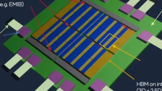
IEDM is always eye opening for the advances of device technology. The 2024 meeting in San Francisco this week has not only shown the latest 2nm CMOS process technologies, but way beyond.
TSMC is discussing the technology for its A16 node at the end of 2026, while European researchers at imec have been showing, and making, the components for a standard cell with stacked CFET nanosheet transistors for A7 in the early 2030s.
While there used to be talk of the ‘end of Moore’s Law’ (and certainly the end of Dennard scaling) Intel has been pushing back.
“We continue to be the stewards of Moore’s Law for the industry,” said Sanjay Natarajan, SVP & GM of the Intel Technology Research Group, the newly renamed Components Research group. “We are releasing groundbreaking new technology,” he said. “We have in my opinion perhaps the strongest research development pipeline in the industry.”
He points to the combination of device technology, interconnect and packaging as vital to driving the technology forward.
To read the full article, click here
Related Chiplet
- DPIQ Tx PICs
- IMDD Tx PICs
- Near-Packaged Optics (NPO) Chiplet Solution
- High Performance Droplet
- Interconnect Chiplet
Related News
- Is Chiplets the Answer to the End of Moore’s Law?
- Enosemi and GlobalFoundries announce the availability of silicon-validated electronic-photonic design IP available in the GF Fotonix platform
- Unveiling the Availability of Industry’s First Silicon-Proven 3nm, 24Gbps UCIe™ IP Subsystem with TSMC CoWoS® Technology
- Hybrid bonding: A global picture of the IP competition
Latest News
- LTSCT Joins imec Automotive Chiplet Program
- CEA-Leti Will Present Its Latest Advances On Next-Generation Chip Integration at ECTC 2026
- OpenLight Secures $50 Million in Series A-1 Funding to Accelerate Global Deployment of Next-Generation Photonics
- Lightmatter Names Roy Kim Vice President of Product to Lead Global Deployment of Photonic Interconnects
- Why Chip Sovereignty Is No Longer About Chips—But Systems