Chiplet Standard Goes 3D
By Gary Hilson, EETimes (September 9, 2024)
The standards governing chiplet technology now have a second iteration.
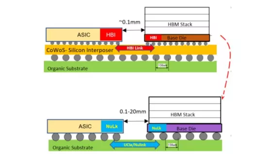
The Universal Chiplet Interconnect Express (UCIe) Consortium, which was formed in March 2022, recently released its 2.0 specification with updates that address design challenges for testability, manageability and debug (DFx) for the SiP lifecycle across multiple chiplets. A key feature of the update is support for 3D packaging to enable chiplets to dramatically increase bandwidth density and power efficiency.
In a briefing with EE Times, consortium chair Debendra Das Sharma said that the UCIe 2.0 specification is fully backward compatible, while introducing optional manageability features and a UCIe DFx Architecture (UDA) that supports vendor agnostic chiplet interoperability.
The consortium has spread work on the specification across several working groups that focus on different aspects, including electrical, protocol, form factor and compliance, manageability and security, and systems and software. Das Sharma said a recently formed automative working group reflects an interest from that sector to start gathering requirements.
To read the full article, click here
Related Chiplet
- DPIQ Tx PICs
- IMDD Tx PICs
- Near-Packaged Optics (NPO) Chiplet Solution
- High Performance Droplet
- Interconnect Chiplet
Related News
- DreamBig Semiconductor Announces Partnership with Samsung Foundry to Launch Chiplets for World Leading MARS Chiplet Platform on 4nm FinFET Process Technology Featuring 3D HBM Integration to Solve Scale-up and Scale-out Limitations of AI for the Masses
- Cadence to Buy Artisan to Support Chiplet, 3D IC Future
- InPsytech Tapes Out F2F SoIC Design Compliant with UCIE 2.0 Standard Enabling High-Speed Interconnects for 3D Heterogeneous Integration
- Keysight Unveils 3D Interconnect Designer for Chiplet and 3DIC Advanced Package Designs
Latest News
- CEA-Leti, CEA-List and PSMC Collaborate to Integrate RISC-V and MicroLED Silicon Photonics into 3D Stacking and Interposer for Next-Generation AI
- NIST Researchers Develop Photonic Chip Packaging That Can Withstand Extreme Environments
- Rebellions Closes $400 Million Pre-IPO and Launches RebelRack™ and RebelPOD™ to Accelerate Global Expansion
- EdgeCortix Looks To Chiplets For Third-Gen Reconfigurable AI Chip
- Agileo Automation Launches Agil'EDA to Accelerate SEMI EDA Adoption for Semiconductor Equipment OEMs