How to Validate Chiplet Designs in the World of AI

The rise of AI and data centers is placing higher performance demands on systems than ever before, which requires increasingly advanced chiplet designs. The need to meet this level of performance has driven the development of new compliance standards for communication between chiplets with advanced packages. These emerging standards, such as Universal Chiplet Interconnect Express (UCIe) 2.0, provide a metric for engineers to validate and analyze their chiplet designs through simulations.
What are the Complexities of Chiplet Design and Signal Integrity?
Verifying the compliance of your package designs before manufacturing can reduce risks, save thousands on prototype costs, and speed time to market. Modeling your design with the help of programs such as Keysight’s Chiplet PHY Designer 2025 gives you key insights into your design’s signal integrity by allowing you to analyze forward clocking and run simulations for Voltage Transfer Function (VTF), insertion loss, return loss, crosstalk, and eye diagrams. This, in turn, gives you the opportunity to refine and optimize your design before incurring material costs.
Achieving low latency and high bandwidth are key goals in chiplet interconnect design, and the UCIe specification provides guidelines for optimizing these parameters.
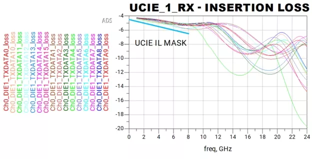
Figure 1: UCIE Die-to-Die Interconnect Insertion Loss Example
The dense interconnects in both chiplet architectures and the UCIe standard pose significant design challenges, especially in regard to crosstalk and simultaneous switching noise (SSN). As signal lines are packed closer together within chiplet designs, instances of unwanted inductive and capacitive coupling increase. The rise in crosstalk often results in corrupt data and degraded signal integrity. Bandwidth density and bump pitch are important factors that influence signal integrity and overall system performance, as shrinking bump pitch can improve bandwidth density but may also increase electrical parasitics and crosstalk. This issue is exacerbated by UCIe's adoption of a single-ended parallel bus, where multiple signals switch concurrently. These simultaneous switching outputs (SSO) generate a substantial amount of SSN, which in turn causes voltage fluctuations on the power and ground planes. Voltage fluctuations can lead to false switching and reduced noise margins, ultimately resulting in system instability and performance degradation.
Sophisticated design techniques, advanced modeling, and innovative packaging solutions are key to mitigating these challenges and ensuring reliable high-speed data transfer within chiplet-based systems. Advanced packaging and interconnect technologies play a crucial role in reducing crosstalk and improving the reliability of chiplet systems by enabling higher interconnect density and better signal integrity. For example, in Figure 2 below, QTYx16 UCIe data eyes are simulated at 16 Gb/s for a standard package design for this die-to-die interconnect. There are clear eye mask violations visible here, which, as shown in this paper, are a result of crosstalk.
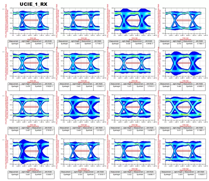
Figure 2: UCIE 16Gb/s Die-to-Die Interconnect Time Domain Simulation Example
With further analysis of the package design and layout, we were able to easily make some package design layout changes to help reduce the crosstalk on the UCIe bus, as shown in Figure 3. Optimizing bump pitch and bandwidth density in these layout changes can also help reduce power consumption in chiplet-based systems.
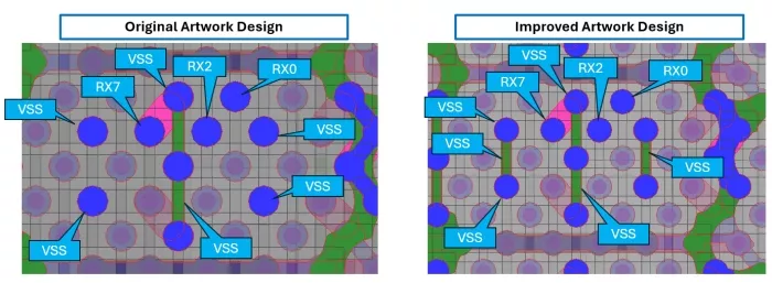
Figure 3: Depiction of Package Layout changes added to mitigate crosstalk in UCIe die-to-die interconnect
In Figure 4, we can see the impact and improvement of these layout changes in terms of crosstalk when looking at a single UCIe bit pulse response.
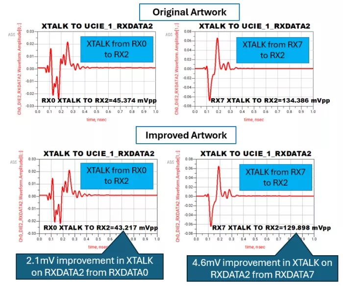
Figure 4: Crosstalk Comparison between the original package design and the improved design to mitigate crosstalk
By looking at Figure 5, which compares results from the initial and improved designs, we can observe the overall improvements in our UCIe data eye time domain response with our complex modeling solutions.
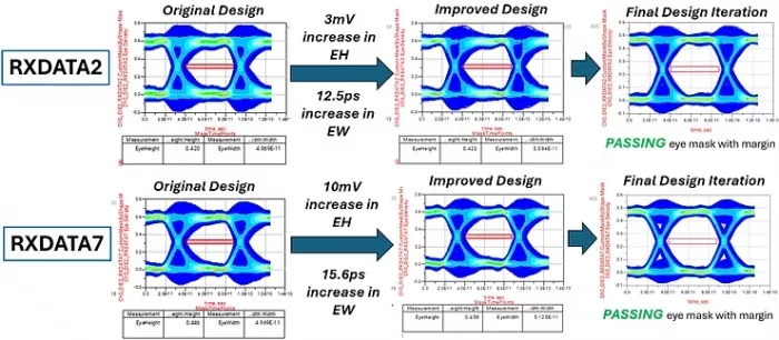
Figure 5: Time Simulation of UCIe Showing Crosstalk Improvements
How Can You Streamline Your Chiplet Validation?
One of the biggest roadblocks to implementing in complex chiplet design modeling for compliance testing is the sheer amount of processing power required to perform these simulations. Maintaining an in-house High Performance Computing Cluster (HPC) can be cost-prohibitive, as they generally run a bill of over $100k. For many labs, the most cost-effective solution is to outsource model generation and simulation, which enables engineers to save on material costs by ensuring compliance in the design stage while avoiding the overhead cost of an in-house HPC.
At Signal Edge Solutions, we specialize in designing, modeling, and integrating solutions for AI applications to meet these compliance standards. We maintain an in-house HPC to support generating complex models and simulations. Our team of packaging and modeling engineers have the expertise to perform complex simulations, measurements, and analyses to help our clients validate their chiplet designs for faster time to market. We even design custom UCIe IBIS models. Reach out to us at info@signaledgesolutions.com about our modeling and measurement services to see how we can help you to optimize your design and be sure that it is hitting the metrics for UCIe compliance standards.
References:
Related Chiplet
- 12nm EURYTION RFK1 - UCIe SP based Ka-Ku Band Chiplet Transceiver
- Interconnect Chiplet
- Bridglets
- Automotive AI Accelerator
- Direct Chiplet Interface
Related Blogs
- Alphawave Semi Bridges from Theory to Reality in Chiplet-Based AI
- The Need for Chiplets, and UCIe in Automotive
- Driving the Development and Deployment of Chiplets in the Automotive Industry
- The Impact of UCIe on Chiplet Design: Lowering Barriers and Driving Innovation
Latest Blogs
- Streamlining Functional Verification for Multi-Die and Chiplet Designs
- Testing At The Speed Of Light: Enabling Scalable Optical Testing For Silicon Photonics And CPO
- How to Validate Chiplet Designs in the World of AI
- The Unfinished Revolution
- Xcelium Distributed Simulation App Accelerates Multi-Die Simulations Up to 3X