Case Study: How to Sign Off Your UCIe Interface

As 3D heterogeneous integration (3DHI) systems increase in complexity, the importance of the Universal Chiplet Interconnect Express (UCIe) standard is becoming critical to the future of advanced packaging and semiconductor system designs that support AI and high-power computing (HPC) applications.
A Cadence webinar featuring Sigrity Signal and Power Integrity offers a comprehensive guide for developing a functional UCIe interface using a Cadence IP test package as an example. An overview of the UCIe interface specification is provided, along with a design and analysis workflow that ensures rapid and accurate compliance with the interface standard. Valuable insights into the integration process of chiplets with UCIe PHYs across various package types are offered, including both organic and silicon substrates. The session concludes with a demonstration in which a UCIe interface is created that meets industry standards, utilizing Cadence's integrated design and analysis tools.
Below is a quick summary of the information you will glean from viewing this webinar on demand.
What Is UCIe and How Can Cadence Customers Check UCIe Compliance?
UCIe is an industry standard that enables high speed, low-latency, and low-power interconnect between packaged chiplets from different manufacturers to work together as a larger system. Cadence has implemented the UCIe specification into the Sigrity SystemSI compliance kit.
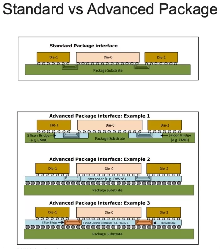
UCIe supports two types of interconnects. When connections embedded in the package substrate are used to connect the two dies, it is called the standard package and results in lower cost, lower connection density, and longer reach. This is also known as the 2D interconnect. Alternatively, an interposer or bridge can be placed between the active dies and package to give a layer of high-density routes, as shown in the image below, or a silicon bridge embedded in the package substrate. This is called an advanced package, which provides a much higher density of connections and lower power consumption, but higher cost and shorter reach. In both cases, UCIe supports a range of speeds, as well as a significantly better bit-error-rate (BER) than chip-to-chip interconnects.
The SystemSI compliance kit supports both the standard and advanced package interfaces as well as the different supported speeds. Once the standard or advanced package template is selected, all the information for the BER and speed is available.
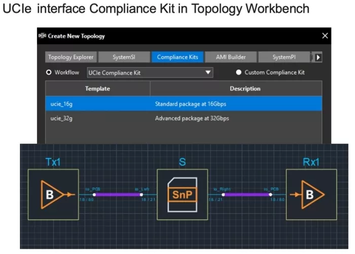
This new UCIe kit includes the UCIe specification for v1.1, as well as templates for data rates of 16 and 32Gbps, generic IBIS-AMI models, a generic UCIe reference channel, voltage transfer function (VTF) calculations, and a compliance check report.
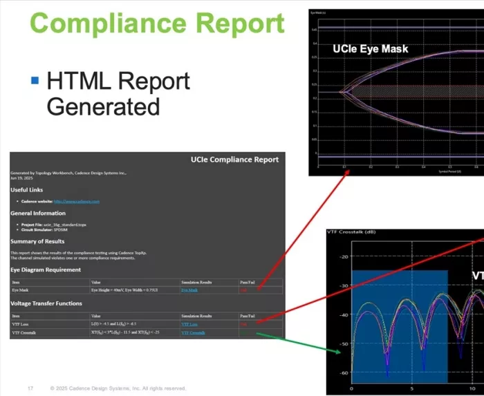
The webinar describes several channel specs, including eye mask requirements, the VTF function, VTF loss, VTF crosstalk, and VTF for standard and advanced packages.
Case Studies from the Cadence UCIe IP Packaging Team
Package technology examples include CoWoS-R/L/S from TSMC, embedded multi-die interconnect bridge (EMIB) from Intel, and fan-out chip-on-substrate (FOCoS) from ASE.
-
Cadence UCIe IP Gen1 (16G – Blizzard) – UCIe AP/SP – Packages: Cadence Expertise
- Package design requirements
- Summary of SI/PI requirements for package design
- M4-M3 metal connections
- Channel and signal analysis
- Die-to-die signal integrity checks
- Signal integrity simulations (SI analysis, simulation setup, analysis, and specification)
- Skew analysis simulation
- Cadence channel 25mm/15mm/5mm channel loss
- Cadence channel 25mm/15mm/5mm crosstalk
- Crosstalk simulation results
- Power integrity analysis
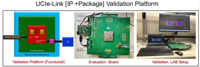
- UCIe Link (IP and Package) Validation Platform
- TX output to scope setup
- 32G TX output eye
- 32G low-swing performance on AB (7.4mm)
Conclusion
Demand for UCIe-compliant devices is on the rise as the cost and complexity of monolithic system on chips (SoCs) continue to impact growth in the heterogeneous integration of chips/chaplets. The UCIe standard is being adopted by many chip manufacturers due to industry standardization, interoperability, modularity, and scalability requirements. The UCIe specification focuses on advanced packaging technologies that support AI and high-power computing (HPC) applications.
View Cadence's "High-Performance Hierarchical IR Signoff for Large SoCs and 3D-ICs" webinar to gain valuable insights into how we can partner with you for UCIe IP as well as for implementing successful die-to-die connectivity. Cadence is your partner for:
Related Chiplet
- Interconnect Chiplet
- 12nm EURYTION RFK1 - UCIe SP based Ka-Ku Band Chiplet Transceiver
- Bridglets
- Automotive AI Accelerator
- Direct Chiplet Interface
Related Blogs
- How to Make Chiplets a Viable Market
- Bring Your Own RTL to Zero ASIC's Chiplet Ecosystem
- How Kandou has been getting ready to unlock AI from day one
- How 40G UCIe IP Powers Data Center AI Chips
Latest Blogs
- 3D-IC Market Outlook: Technology Roadmaps, Readiness, and Design Implications
- Cadence 3D-IC Success Stories: Faster Bandwidth, Lower Power, On-Time Tapeouts
- 3D-IC Test and Reliability: KGD Strategies, Access Architecture, & Failure Mode
- 3D-IC in AI, HPC, and 5G: Bandwidth, Latency, and Energy per Bit Advantages
- Bosch and the chiplet revolution: Enabling software-defined mobility