Co-Optimization of Power Delivery Network Design for 3-D Heterogeneous Integration of RRAM-Based Compute In-Memory Accelerators
By Madison Manley, James Read, Ankit Kaul, Shimeng Yu and Muhannad Bakir
Department of Electrical and Computer Engineering, Georgia Institute of Technology, Atlanta, GA 30332 USA
ABSTRACT
Three-dimensional heterogeneous integration (3D-HI) offers promising solutions for incorporating substantial embedded memory into cutting-edge analog compute-in-memory (CIM) AI accelerators, addressing the need for on-chip acceleration of large AI models. However, this approach faces challenges with power supply noise (PSN) margins due to VDD scaling and increased power delivery network (PDN) impedance. This study demonstrates the necessity and benefits of 3D-HI for large-scale CIM accelerators, where 2-D implementations would exceed manufacturing reticle limits. Our 3-D designs achieve 39% higher energy efficiency, 8× higher operation density, and improved throughput through shorter vertical interconnects. We quantify steady-state IR-drop impacts in 3D-HI CIM architectures using a framework that combines PDN modeling, 3D-HI power, performance, area estimation, and behavioral modeling. We demonstrate that a drop in supply voltage to CIM arrays increases sensitivity to process, voltage, and temperature (PVT) noise. Using our framework, we model IR-drop and simulate its impact on the accuracy of ResNet-50 and ResNet-152 when classifying images from the ImageNet 1k dataset in the presence of injected PVT noise. We analyze the impact of through-silicon via (TSV) design and placement to optimize the IR-drop and classification accuracy. For ResNet architectures in 3-D integration, we demonstrate that peripheral TSV placement provides an optimal balance between interconnect complexity and performance, achieving IR-drop below 10% of VDD while maintaining high classification accuracy.
INDEX TERMS
3-D heterogeneous integration (3D-HI), compute-in-memory (CIM), emerging nonvolatile memory (eNVM), IR-drop, power delivery network (PDN), RRAM reliability.
I. INTRODUCTION
The number of parameters in machine-learning models continue to grow exponentially [1], leading to increased power densities to run large computing workloads and challenges in designing energy-efficient architectures [2]. Compute-in-memory (CIM) has been proposed to address these challenges by reducing data movement and increasing parallelism in DNN computations. CIM cores efficiently compute vector-matrix multiplications (VMMs) in highly parallel analog circuits, forming the basis for DNN accelerators. Emerging nonvolatile memories (eNVMs), such as resistive random access memory (RRAM), ferroelectric memories (transistor/capacitor), phase change memory (PCM), and magnetic random access memory (MRAM) are potential CIM weight elements due to their higher bit density (compared to SRAM at the same tech node) and low leakage (for dynamic power gating). This enables large on-chip memory capacity and high energy-efficiency. These architectures perform optimally when neural network parameters are written once to nonvolatile memory, eliminating the energy costs of repeated data movement while enabling efficient analog computations. However, networks larger than 75 MB at legacy nodes (>22 nm) require die sizes >1000 mm2. This was estimated using NeuroSim [3], an open-source automated framework for PPA analysis of CIM accelerators. Using ResNet-50 (a 76 MB network) and the parameters listed in Table 1, a 2-D design at 22 nm node exceeds 1000mm2. This is infeasible given today’s reticle size limit of 858mm2 without techniques like reticles titching. In addition to large die sizes, the growing demand to provide higher logic-memory bandwidth and lower die-to-die signal inter-connection delay has led to a technological push toward 3-D heterogeneous integration (3D-HI) architectures, such as through-silicon via (TSV)-based 3-D integrated circuits (ICs) [4], [5], [6]. The 3D-HI of chiplets is critical to enable higher compute density and signaling energy-per-bit through a reduced footprint and interconnect length for state-of-the-art CIM hardware accelerators [7]. Although 3D-HI can potentially enhance the bandwidth, throughput, and latency of the system, delivering power to multitiered CIM systems presents challenges.
Device scaling and reducing hardware form-factor are effective methods to improve energy and compute efficiency in low-power edge applications. However, these approaches introduce significant challenges for power delivery design. As hardware shrinks, the area for edge intelligent components and voltage regulators decreases, necessitating the miniaturization of power delivery components such as interconnects, capacitors, and inductors. This miniaturization, coupled with increasing power density in recent CIM and hardware accelerators [8], complicates power delivery design. Recent work has shown that parallel vector-matrix-multiplication on multiple CIM cores can introduce nonidealities like core-to-core variation of IR-drop and supply voltage instability [9]. 3D-HI exacerbates these challenges.
While TSV-based 3D-HI technologies reduce area com-paredto2-Dcounterparts,power requirements remain similar despite fewer power delivery interconnects [10]. Limited vertical routing resources can drastically increase steady-state power supply noise (PSN). Additionally, power must travel through highly resistive paths including on-die power delivery networks (PDNs), through-silicon-vias (TSVs), and I/O bumps, contributing to high IR-drop [11]. High IR-drop can significantly affect 3-D CIM system reliability and performance. A large drop in supply voltage across RRAM memory arrays introduces read instability and variations in analog outputs. The nonuniform voltage distribution across memory blocks exacerbates these issues, leading to incorrect computations [9]. In addition, peripheral circuits such as ADCs, are sensitive to IR-drop and voltage instability can degrade performance due to increased sensing errors. These errors significantly impact the CIM inference accuracy, potentially degrading the performance of AI algorithms. Therefore, addressing these power delivery challenges is essential for realizing the full potential of scaled-down, energy-efficient edge AI hardware using 3D-HI architectures.
To address the interdisciplinary challenges of power delivery in 3D-HI RRAM-based CIM technologies, we propose a co-design methodology. The key contributions of this article include.
1) A rapid analysis flow enabling early design-space exploration of power delivery parameters and their impact on CIM performance metrics for early-stage prototyping to evaluate design trade-offs.
2) A comprehensive benchmarking of TSV-based 3-D integration (7-nm CMOS logic and 22-nm RRAM memory) against monolithic 2-D designs, resulting in an optimized 3-D integration approach that maximizes CIM inference accuracy.
II. COMPARATIVE ANALYSIS: 3-D VERSUS 2-D CIM ARCHITECTURES
To evaluate the performance and area trade-offs between 2-D and 3-D architectures for CIM, we developed a TSV-based 3-D-integrated model of an analog CIM accelerator. Our study focuses on 3-D designs that combine 7-nm logic and 22-nm RRAM memory, applied to a pretrained ResNet-50 and ResNet-152 models [1] using the ImageNet 1k dataset. We used TensorRT’s quantization framework [12] to quantize the model to 8-bit inputs and weights, enhancing computational efficiency while maintaining accuracy. Our architecture adopts a pipelined approach that allows parallel execution of all memory arrays [3]. This design choice results in low-latency classification times, crucial for real-time applications. The 3-D stack is arranged with tiers on the package substrate, topped by multiple memory tiers that form a memory cube. This configuration aims to optimize both performance and power delivery.
In Fig. 1, we show the 2-D baseline and 3-D architecture configurations. Through this comparison, we aim to quantify the benefits and challenges of 3-D integration for CIM architectures, particularly in terms of power delivery, area efficiency, and inference accuracy. We evaluate the CIM accelerator model using 1 µm diameter TSV in Table 1. We used the 3D NeuroSim simulator to estimate performance projection for heterogeneously integrated CIM accelerators [13]. For the 3-D architecture, the memory blocks (RRAM sub-arrays and switch matrices) are assumed at 22 nm (based on availability from industry, e.g., TSMC and Intel’s latest RRAM processes [14]) and the logic blocks (ADCs and peripherals) are assumed at 7 nm to leverage the scaling benefits. We note that although ADCs are mixed signal circuits, they can be implemented with scaled logic transistors, so they are included in the logic blocks. For the 2-D baseline, the logic blocks are scaled from 7 to 22 nm to consider both logic and memory at 22 nm. The total number of operations (total computations needed architecturally to complete an inference workload) were assumed to be the same for the 2-D and 3-D design. As shown in Table 1, the energy efficiency (TOPS/W) is observed to be 39% higher and the operation-density (TOPS/mm2) is 8× with a 3-D implementation versus 2-D.
TABLE 1. PPA comparison between 2-D and H3-D ResNet-152 accelerators.
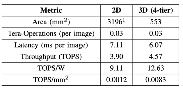
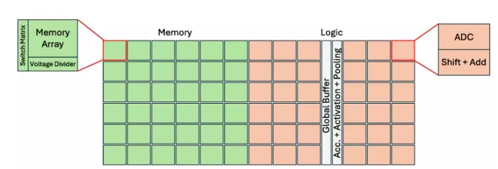
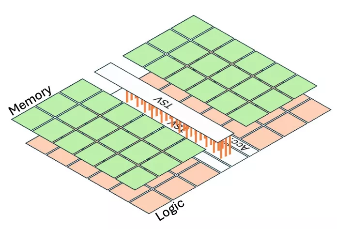
FIGURE 1. CIM architecture configurations for (a) 2-D and (b) 3-D layer by layer (3D) with a localized TSV design.
III. THREE-DIMENSIONAL CIM PSN EVALUATION METHODOLOGY FROM DEVICE/INTEGRATION TOWARD APPLICATION LEVEL
To assess the impact of 3D-HI PDN design parameters on inference accuracy, we have developed an integrated methodology, as illustrated in Fig. 2. Our evaluation framework consists of three key stages that bridge device-level effects to system-level performance. The power analysis stage uses DNN + NeuroSim to map neural networks to memory arrays, calculating detailed power profiles and determining current draw patterns based on network architecture and mapping. The PDN modeling stage applies these power profiles to analyze voltage distributions using finite-difference methods for steady-state IR-drop analysis, modeling package-level to on-diePDNeffectsacrossthe3-Dstack.Theaccuracyimpact analysis stage then simulates voltage variation effects on analog computations, models ADC conversion considering supply-dependent reference voltages, and evaluates end-to-end network accuracy with these nonidealities.
This approach enables rapid prototype analysis for initial design development, balancing computational speed with accuracy. By integrating these stages, we can directly correlate PDN characteristics with CIM performance metrics. This approach captures the relationships between power delivery and computational accuracy in 3D-HI CIM architectures.
Although this study primarily focuses on steady-state IR-drop analysis, our framework also supports transient-state analysis. For our designs, we assume an operating frequency of100MHz[14]. At this frequency, the switching speed of the digital circuits is low, reducing the impact of dynamics witching noise. Additionally, all digital circuits are placed on the bottom tiers to avoid inductance parasitics from TSVs. With these assumptions, the impedance of the PDN becomes the dominant noise contributor. The following sections provide a detailed description of each component and their integration, offering insights into how PDN design choices influence the overall system performance.
A. THREE-DIMENSIONAL PDN MODELING METHODOLOGY
To model the steady-state IR-drop of the 3-D CIM architecture, we implement a distributed package-level PDN model to reflect the spreading effects of current in the package and the coupling between different P/G bumps based on and validated on IBM opensource benchmarks for steady-state and transient-state [15]. We used this framework to model steady-state IR-drop for the two-tier ResNet-50 and four-tier ResNet-152 integration architectures shown in Fig. 3 with TSV distributions shown in Fig. 4. The resistance net-work models of the board, package, and on-die PDNs are first generated, then subsequently combined to solve for nodal voltages and branch currents. An ideal voltage regulator module (VRM) is assumed for board-level PDN and a lumped resistance network is used to model board-level current spreading. The package power/ground planes are modeled as two layers with the bottom layer connected to the motherboard with ball grid arrays (BGAs) and the top layer connected to the on-die PDN through C4 bumps. Each node in the two layer network is connected to six adjacent nodes through a resistance, representing either package traces or interlayer vias.
The on-die PDN consists of multiple metal layers with parallel P/G wires within each layer and orthogonal wiring between adjacent layers. To capture both the interleaved PDN structure and the effect of on-die vias, we model the on-die PDN as a two-layer resistance network. The metal wires on each on-die PDN are typically uniformly distributed, but if the actual layout is nonuniform, we calculate the effective wire pitch and via density to reorganize the PDN layout. For each on-die layer, we map fine-granularity PDN layout to coarse mesh grids at a microbump granularity. The equivalent parallel resistance is calculated for each coarse grid containing multiple vias and metal wires and assigned using models described in [15]. All coarse PDN layers with x-axis and y-axis metal wires are mapped onto the top and bottom layers, respectively.
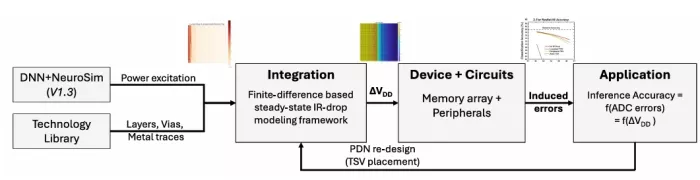
FIGURE 2. Three-dimensional CIM PSN evaluation and co-design methodology.
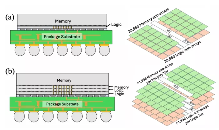
FIGURE 3. Cross section and tier breakdown of (a) two-tier ResNet-50 architecture and (b) four-tier ResNet-152 architecture.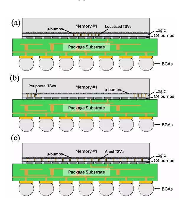
FIGURE 4. Cross section of the two-tier integration architecture for PDN evaluation for (a) localized TSV distribution, (b) peripheral TSV distribution, and (c) areal TSV distribution.
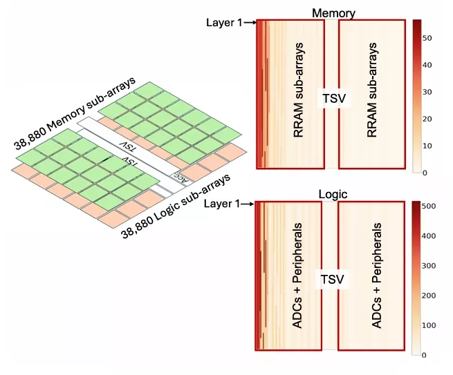
FIGURE 5. Current map of the memory and logic tier of the two-tier ResNet-50 integration architecture.
B. INFERENCE ACCURACY AND PPA ESTIMATION
Our evaluation of the 3D-HI CIM architecture utilizes 3-D NeuroSim [15] for chip design and initial simulations of area, power, and latency. This tool automatically maps the convolutional and linear layers of the neural network to memory arrays and calculates the current draw for each array, as illustrated in Fig. 5. The early layers of ResNet-like net-works have dense input and weight feature maps compared to the later layers, resulting in a higher power in the early arrays during computation. Dense feature maps activate more RRAM arrays, increasing current draw and IR-drop. Using a column-major mapping scheme, early layers are mapped to the leftmost edge of the memory tier, creating hotspots along this edge. These current maps are used as input to our PDN model, enabling simulation of IR drop across various design configurations. To demonstrate the area savings of splitting the logic and memory components into different tiers, Fig. 6 shows an area breakdown between the 2-D baseline entirely in the 22 nm node and a hypothetical 2-D design with the logic components in the 7 nm node.
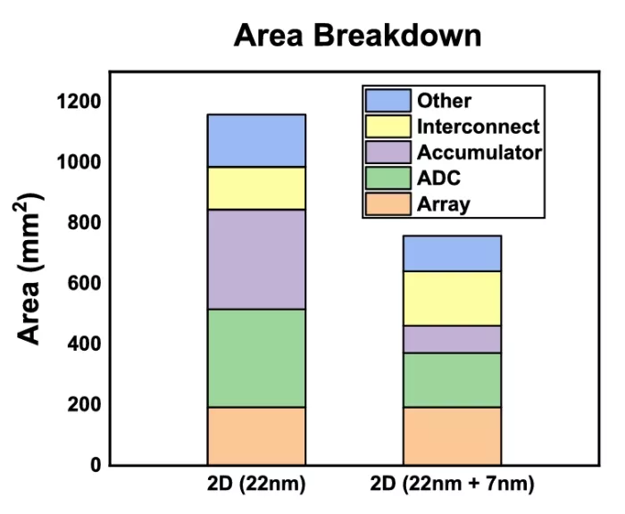
FIGURE 6. Area breakdown for the hypothetical 2-D baseline design and a hypothetical 7 + 22 nm 2-D design. By moving the expensive accumulator and ADC circuits to a more advanced node, the area is reduced by 35%.
To accurately assess the impact of nonideal effects on analog computations, we developed a detailed behavioral simulator. This simulator incorporates a GPU-accelerated circuit solver for analog computation simulation that integrates with 3-D NeuroSim for automated chip design and includes a functional simulator for DNN inference that is compatible with pretrained PyTorch models. Our simulation process begins by quantizing inputs and weights to 8-bit integers and mapping DNN layers to memory arrays as determined by NeuroSim. We then simulate each array’s behavior using PyTorch to leverage GPU acceleration. For each memory array, our simulation maps the 8-bit integer weights to the RRAM conductances, converts the inputs to binary voltage sequences, and applies the input vectors to the input wires. Then, it calculates currents through each RRAM, representing the analog multiplication, and sums currents along the output wires which represent the analog weighted sum operation. The output current is then converted to a voltage using a voltage divider circuit. Finally, the 7-bit ADC process is simulated by converting the output voltages to a digital code by comparing the output with a series of 128 reference voltages generated by reference memory arrays (Fig. 7).
To capture real-world behavior, we integrate models of nonideal effects into our simulation. IR-drop is incorporated by modulating the supply voltage in each array using results from our PDN model. IR-drop reduces the supply voltage to the arrays, which reduces the output signal range. This in turn decreases the margin between analog output states which leads to higher sensitivity to other noise sources. To study IR-drop’s effect on noise sensitivity, we inject noise to the analog output voltages following a simplified Gaussian noise model, representing process, voltage, and temperature (PVT) noise. This approach allows us to isolate and study the impact of IR-drop under consistent noise conditions. Transient noise is not explicitly incorporated in this simulation due to the 100 MHz operating frequency discussed previously.
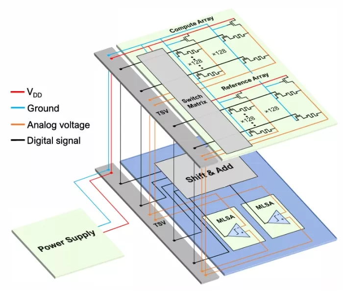
FIGURE 7. Circuitry split between memory tiers (top) and logic tiers (bottom). Area intensive circuits such as shift-adders, accumulators, and sense amplifiers are placed in more advanced process node to save area. RRAMs and necessary peripherals are kept in the most advanced RRAM process node.
This framework allows us to rapidly quantify how choices in the TSV design interact with chip hotspots that arise from DNN workloads and affect overall chip performance.
C. EXPERIMENTAL SETUP
The key parameters of our PDN model and device/circuit specifications are summarized in Table 2. We evaluate the impact of IR-drop and classification accuracy on ResNet-50 and ResNet-152 for three different TSV configurations.
1) A localized TSV distribution with TSVs based on high bandwidth memory designs with TSVs concentrated in the center of the die [6], [16].
2) A peripheral TSV distribution where power TSVs are located along the edges of the die.
3) An areal TSV distribution where TSVs are evenly distributed across the die area.
We analyze each TSV configuration to understand the trade-offs in interconnect design and mitigating IR-drop and optimizing classification accuracy.
The 3-D designs use a memory-on-logic approach, with memory at 22 nm and logic at 7 nm, in the two-tier and four-tier designs. For the two-tier design, the memory and logic die each have 38880 sub-arrays. We split the memory and logic dies for the ResNet-152 network due to the size of the individual dies that are beyond the reticle limit. The memory and logic dies are split into two chiplets, with each chiplethaving51696sub-arrays. We strategically arrange the chiplets by placing the high-powered logic chiplets near the bottom of the stack to be closer to the power source and low-powered memory chiplets near the top of the stack to minimize the IR-drop. For all TSV configurations, we assume a 1 µm diameter and 10:1 aspect ratio. To ensure that the total number of TSVs remain constant between all designs, we vary the TSV pitch.
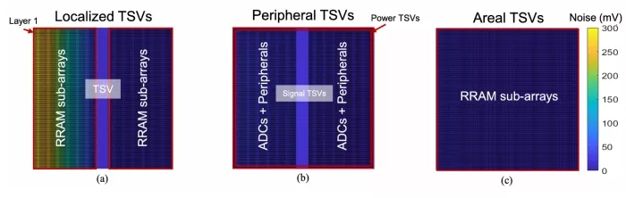
FIGURE 8. IR-drop contours for two-tier ResNet-50 integration architecture for (a) localized TSV configuration, (b) peripheral TSV configuration, and (c) areal TSV configuration.
For CIM-based inference, we use 1-bit per cell RRAM[14] and the ResNet-50 and ResNet-152 network trained on ImageNet-1k. We followed NeuroSim’s [3] process for chip floorplan and mapping. The chip executes in a pipelined fashion, allowing each layer to compute in parallel. To optimize throughput of the chip, we duplicate the weights in layers with large input feature maps. This avoids creating bottlenecks in the pipeline at the expense of larger chip area and power. This accounts for the larger memory capacity on-chip than weight size of ResNet-50 in Table 2. Fig. 5 shows current maps for logic and memory tiers in both the naive and optimized two-tier configurations. Table 3 provides the tier-level power breakdown for each architecture.
We assume 7-bit multilevel sense amplifiers are used to sense analog outputs at the columns of each array. Because the logic tier is at a more advanced node, we can afford to include 1 ADC per column in each RRAM array, improving throughput compared to a homogeneous design where ADCs are commonly shared among multiple columns to limit their area overhead.
IV. RESULTS
A. STEADY-STATE IR-DROP ANALYSIS OF 3-D CIM CONFIGURATIONS
Two-tier ResNet-50 and four-tier ResNet-152 integration architecture were considered for three different TSV configurations. Fig. 8 depicts the IR-drop contours of the memory tier of the two-tier ResNet-50 architecture for the three TSV designs. Fig. 9 summarizes the maximum IR-drop for each TSV configuration relative to the 2-D baseline.
TABLE 2. PDN, device, and neural network parameters.
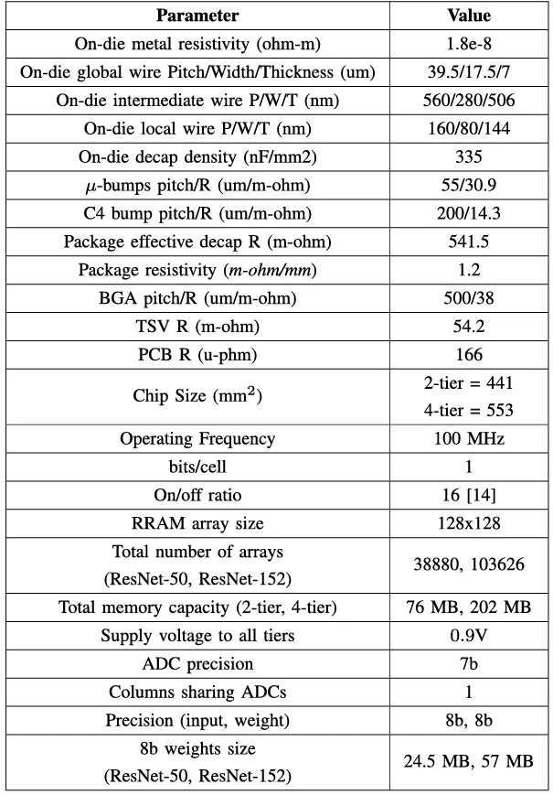
TABLE 3. Tier-level power breakdown.

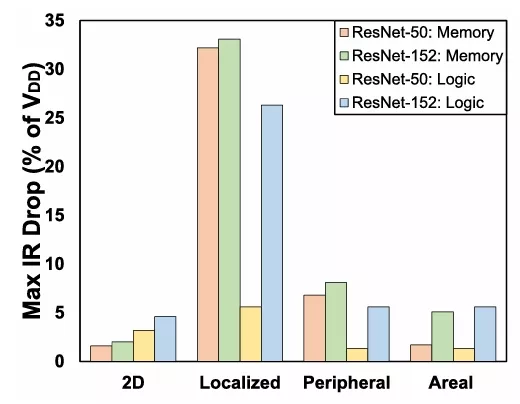
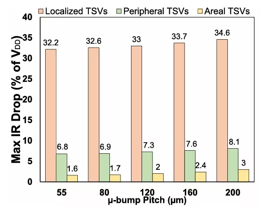
FIGURE 9. (a) Maximum IR-drop as % of VDD for the ResNet-50 and ResNet-152 integration architectures for the three considered TSV designs and (b) maximum IR-drop of the memory tier for the ResNet-50 architecture versus microbump pitch.
The two-tier architecture shows a significant increase in memorytierIR-dropwhenmovingfrom2-Dto3-Dlocalized TSV configuration, with worst-case noise increasing from ≈2% of VDD to 32%, respectively. This increase stems from the combined resistance of the TSVs and the memory tier’s on-die PDN. Furthermore, placing the high-power memory blocks near the edge of the die is the worst-case scenario for localized TSV designs, as this exacerbates the noise due to the high currents that are required to go through the highly resistive memory PDN. Similarly, the four-tier ResNet-152 localized TSV design also has a significant increase in the IR-drop for both memory and logic due to partitioning mem-ory and logic into multiple chiplets. It is also important to observe that the difference in IR-drop between the memory and logic blocks is significant for the localized 3-D designs. This behavior has a negative impact on the CIM inference accuracy, which is discussed in Section IV-B.To mitigate the IR-drop of the localized TSV design, we analyze a peripheral and an areal TSV configuration. With a peripheral TSV design, the noise of the memory tier drops to 6.8% and 8% of VDD for the two-tier and four-tier design, respectively. A large decrease in IR-drop is also observed for the logic tier for the ResNet-152 architecture. This TSV configuration is an effective method to reduce the maximum IR-drop for our design assumptions. By placing the high-powered sub-arrays along the edges of the die, the path of resistance the high currents are required to travel through is significantly reduced. It is important to note that because of our specific design, the peripheral TSV distribution significantly reduces the IR-drop compared to the localized TSV distribution. However, if the high-powered sub-arrays are located in the center of the dies, the IR-drop will suffer with a peripheral TSV design. We analyze an areal TSV configuration for ResNet-50 and observe an IR-drop of 1.7% of VDD for the memory tier and 5.1% of VDD and 4.9% of VDD for the memory and logic tier for ResNet-152. This TSV configuration results in the lowest IR-drop, however, an areal TSV distribution can lead to increased routing complexity and have a larger keep-out-zone area overhead compared to the localized and peripheral TSV designs. Although there is not a large decrease in IR-drop compared to the peripheral TSV distribution, this TSV design may be optimal for more uniform and dense computations, such as generative AI workloads. Finally, in Fig. 9(b), we analyze the impact of µ-bump pitch on the IR-drop for the integration architectures. We observe that as we decrease the µ-bump pitch, the IR-drop decreases. As expected, as µ-bump density increases, the IR-drop will reduce for all TSV designs. We find that the optimization of TSV interconnect placement contributes significantly more to reducing the IR-drop than µ-bump pitch scaling. For our ResNet integration architectures and assumptions, we determine the peripheral TSV design as the optimal interconnect design.
B. IMPACT OF IR-DROP ON CIM INFERENCE ACCURACY
To quantify the impact of the different TSV designs on the classification accuracy, we incorporated the IR-drop effects of each design into 3-D NeuroSim. Here, we injected Gaussian noise to the analog outputs (voltages) of each memory array to emulate noise from PVT variations. The noise amplitude is represented as a percentage of the linear output sensing margin(7mV)—the voltage difference between adjacent digital levels in the ADC that determines its ability to distinguish different analog values reliably. To capture a wide range of potential noise scenarios, we swept the 3-σ (three standard deviations) value of the injected noise.
Fig. 10 shows the accuracy results of each TSV design for the two-tier ResNet-50 and the four-tier ResNet-152 architectures. In both architectures, the localized TSV distribution results in the largest accuracy drop. This occurs because high-power sub-arrays at the chip’s edge must connect to centrally located TSVs through a long resistive path, leading to worst case IR-drop. The accuracy of ResNet-50 suffers more than ResNet-152 with localized TSVs, with the accuracy quickly dropping to 0% as the injected noise is increased, suggesting that ResNet-50 is more sensitive to noise in the first few layers. Because the localized TSV design results in high IR-drop

FIGURE 10. Impact of TSV placement on inference accuracy (a) ResNet-50 on two-tier design (22 nm RRAM tier + 7 nm logic tier) and (b) ResNet-152 on four-tier design (two 22 nm RRAM tiers + two 7 nm logic tiers). TSV configurations are compared to ideal no IR-drop case. Injected Gaussian noise in analog outputs is shown as percentage of ADC sense margin, demonstrating PDN topology effects on PVT sensitivity.
in the early layers, the number of errors in their calculation will be higher. We see that for this design, the accuracy drops 8% and 3% from the baselines at 3σ = 32% for ResNet-50 and ResNet-152, respectively. This indicates ResNet-50’s higher sensitivity to early-layer errors compared to its larger counterpart. ResNet-152 experiences larger accuracy drops across all TSV designs due to higher IR-drop compared to ResNet-50 [Fig. 9(a)]. This is explained by the larger cur-rent demands of the model and the impact of increasing the number of stacked dies in the architecture. While areal TSV distribution achieves highest accuracy, peripheral TSV placement offers a practical compromise between performance and design complexity. We achieve an IR-drop less than 10% of VDD while maintaining high accuracy, avoiding overly complex and more expensive solutions. This highlights the importance of co-optimization between interconnect design and CIM accuracy. For workloads with dense layers in the beginning/end of a network like ResNets, a peripheral TSV design offers the best accuracy and most cost-effective integration.
C. THERMAL IMPACT OF 3-D CIM
TSV-based 3D-HI architectures typically have higher max junction temperatures compared to monolithic 2-D archi-tectures due to interdie coupling and increased junction-to-ambient thermal resistance of the stack. Thermal-induced conductance drift is a challenge for RRAMs, which can affect CIM inference accuracy and reliability [8], [17]. We evaluate the thermal performance of our two-tier and four-tier 3-D CIM designs using Ansys Mechanical with power assumptions in Table 3. We assume an air-cooled heat sink with a convection coefficient of 2000 W/m2 · K. For our design assumptions, we find that the two-tier and four-tier architectures have a maximum junction temperature of 45.5 ◦C and 65.4 ◦C, respectively. Therefore, the 3-D stacking of our proposed architectures do not significantly affect the RRAM devices, as RRAM reliability is largely impacted by temperatures over 100 ◦C [18]. However, with larger networks that require higher power densities, 3-D stacking can lead to significant thermal issues. Therefore, a more comprehensive and detailed multiphysics electrical thermal co-analysis is planned for future work.
V. CONCLUSION
This study investigated power delivery challenges in 3D-HI CIM architectures for AI accelerators. An integrated methodology was developed for early PDN design space exploration to bridge interconnect design and CIM accuracy for rapid prototyping. For our ResNet-50 and ResNet-152 integration architectures and design assumptions, we found a peripheral TSV distribution is the most optimal interconnect design, achieving a balance between IR-drop and classification accuracy. This design was effective in minimizing the IR-drop while maintaining high classification accuracy. This research opens possibilities for 3-D integrated AI accelerators. Looking ahead, applying this methodology to larger models could enable efficient hardware implementations for large language models.
REFERENCES
[1] K. He, X. Zhang, S. Ren, and J. Sun, ‘‘Deep residual learning for image recognition,’’ in Proc. IEEE Conference on Computer Vision Pattern Recognition (CVPR), Las Vegas, NV, USA, Jun. 2016, pp. 770–778, doi: 10.1109/CVPR.2016.90.
[2] L. Su, ‘‘Opening plenary speaker—Delivering the future of high-performance computing,’’ in Proc. Hot Chips 31, Palo Alto, CA, USA, 2019.
[3] X. Peng, S. Huang, Y. Luo, X. Sun, and S. Yu, ‘‘DNN+NeuroSim: An end-to-end benchmarking framework for compute-in-memory accelerators with versatile device technologies,’’ in IEDM Tech. Dig., Dec. 2019, p. 32, doi: 10.1109/IEDM19573.2019.8993491.
[4] S. Sinha et al., ‘‘A high-density logic-on-logic 3DIC design using face-to-face hybrid wafer-bonding on 12nm FinFET process,’’ in IEDM Tech. Dig., San Francisco, CA, USA, Dec. 2020, p. 15, doi: 10.1109/IEDM13553.2020.9372120.
[5] W. Gomes et al., ‘‘Lakefield and mobility compute: A 3D stacked 10 nm and 22FFL hybrid processor system in 12×12 mm2, 1 mm package-on-package,’’ in IEEE Int. Solid-State Circuits Conf. (ISSCC) Dig. Tech. Papers, San Francisco, CA, USA, Feb. 2020, pp. 144–146, doi: 10.1109/ISSCC19947.2020.9062957.
[6] J. C. Lee et al., ‘‘High bandwidth memory(HBM) with TSV technique,’’ in Proc. Int. SoC Design Conf. (ISOCC), Jeju, Korea (South), 2016, pp. 181–182, doi: 10.1109/ISOCC.2016.7799847.
[7] Heterogeneous Integration Roadmap—Chapter 2: High Performance Computing and Data Centers. Accessed: Jun. 28, 2024. [Online]. Available: https://eps.ieee.org/images/files/HIR 2021/ch02hpc.pdf
[8] A. Kaul et al., ‘‘3-D heterogeneous integration of RRAM-based compute-in-memory: Impact of integration parameters on inference accuracy,’’ IEEE Trans. Electron Devices, vol. 70, no. 2, pp. 485–492, Feb. 2023, doi: 10.1109/TED.2022.3231570.
[9] W. Wan et al., ‘‘A compute-in-memory chip based on resistive random-access memory,’’ Nature, vol. 608, no. 7923, pp. 504–512, 2022, doi: 10.1038/s41586-022-04992-8.
[10] S. Sinha, X. Xu, M. Bhargava, S. Das, B. Cline, and G. Yeric, ‘‘Stack up your chips: Betting on 3D integration to augment Moore’s law scaling,’’ 2020, arXiv:2005.10866.
[11] J. Shi, M. Li, and C. A. Moritz, ‘‘Power-delivery network in 3D ICs: Monolithic 3D vs. skybridge 3D CMOS,’’ in Proc. IEEE/ACM Int. Symp. Anoscale Architectures, Jul. 2017, pp. 73–78.
[12] R. Rao et al. (2023). TensorRT GitHub Repository. [Online]. Available: https://github.com/NVIDIA/TensorRT
[13] X. Peng, A. Kaul, M. S. Bakir, and S. Yu, ‘‘Heterogeneous 3-D integration of multitier compute-in-memory accelerators: An electrical-thermal co-design,’’ IEEE Trans. Electron Devices, vol. 68, no. 11, pp. 5598–5605, Nov. 2021, doi: 10.1109/TED.2021.3111857.
[14] P. Jain et al., ‘‘A 3.6Mb 10.1Mb/mm2 embedded non-volatile ReRAM macro in 22 nm FinFET technology with adaptive forming/set/reset schemes yielding down to 0.5 V with sensing time of 5ns at 0.7 V,’’ in IEEE Int. Solid-State Circuits Conf. (ISSCC) Dig. Tech. Papers, Feb. 2019, pp. 212–214.
[15] Y. Zhang, M. O. Hossen, and M. S. Bakir, ‘‘Power delivery network modeling and benchmarking for emerging heterogeneous integration tech-nologies,’’ IEEE Trans. Compon., Packag., Manuf. Technol., vol. 9, no. 9, pp. 1825–1834, Sep. 2019, doi: 10.1109/TCPMT.2019.2931568.
[16] D. U. Lee et al., ‘‘Design considerations of HBM stacked DRAM and the memory architecture extension,’’ in Proc. IEEE Custom Integr. Circuits Conf. (CICC), San Jose, CA, USA, Sep. 2015, pp. 1–8, doi: 10.1109/CICC.2015.7338357.
[17] M. Lanza et al., ‘‘Recommended methods to study resistive switching devices,’’ Adv. Electron. Mater., vol. 5, no. 1, Jan. 2019, Art. no. 1800143.
[18] Z. Fang et al., ‘‘Temperature instability of resistive switching on HfOx-based RRAM devices,’’ IEEE Electron Device Lett., vol. 31, no. 5, pp. 476–478, May 2010.
1 This is a hypothetical 2-D design. Die sizes >858 mm2 require techniques such as reticle stitching to realize.
Related Chiplet
- DPIQ Tx PICs
- IMDD Tx PICs
- Near-Packaged Optics (NPO) Chiplet Solution
- High Performance Droplet
- Interconnect Chiplet
Related Technical Papers
- 3D Stacked HBM and Compute Accelerators for LLM: Optimizing Thermal Management and Power Delivery Efficiency
- A3D-MoE: Acceleration of Large Language Models with Mixture of Experts via 3D Heterogeneous Integration
- Energy-/Carbon-Aware Evaluation and Optimization of 3-D IC Architecture With Digital Compute-in-Memory Designs
- Workflows for tackling heterogeneous integration of chiplets for 2.5D/3D semiconductor packaging
Latest Technical Papers
- In-SoIC ESD Protection for Chiplet-Based 3D Microsystems: Future Research Directions
- ODIN-Based CPU-GPU Architecture with Replay-Driven Simulation and Emulation
- Chipmunq: Fault-Tolerant Compiler for Chiplet Quantum Architectures
- LEXI: Lossless Exponent Coding for Efficient Inter-Chiplet Communication in Hybrid LLMs
- Link Quality Aware Pathfinding for Chiplet Interconnects