DiffChip: Thermally Aware Chip Placement with Automatic Differentiation
Giuseppe Romano 1, Aakrati Jain 2, Nima Dehmamy 3, Cheng ChiI 2, Xin Zhang 2
1 Institute for Soldier Nanotechnologies, Massachusetts Institute of Technology, Cambridge, USA
2 IBM T.J. Watson Research Center, Yorktown Heights, NY, USA
3 MIT-IBM Watson AI Lab, Cambridge, MA, USA
Abstract
Chiplets are modular integrated circuits that can be combined to form a larger system, offering flexibility and performance enhancements. However, their dense packing often leads to significant thermal management challenges, requiring careful floorplanning to ensure efficient heat distribution. To address thermal considerations, layout optimization algorithms concurrently minimize the total wirelength and the maximum temperature. However, these efforts employ gradient-free approaches, such as simulated annealing, which suffer from poor scaling and slow convergence. In this paper, we propose DiffChip, a chiplet placement algorithm based on automatic differentiation (AD). The proposed framework relies on a differentiable thermal solver that computes the sensitivity of the temperature map with respect to the positions of the chiplets. Regularization strategies for peak temperature, heat sources, and material properties enable end-to-end differentiability, allowing for gradient-based optimization. We apply DiffChip to optimize a layout where the total wirelength is minimized while keeping the maximum temperature below a desired threshold. By leveraging AD and physics-aware optimization, our approach accelerates the design process of microelectronic systems, exceeding traditional trial-and-error and gradient-free methods.
Index Terms:
2.5-D integrated circuits (ICs), chiplet floorplanning, computer architecture, hardware/software co-design.
I. Introduction
The exponential increase in device density, as predicted by Moore’s Law [1], has been a key driver of technological advancement. However, this increase necessitates finer lithography techniques, leading to higher manufacturing costs. To address these limitations, chiplets have emerged as a promising solution. They enable efficient scaling by integrating heterogeneous components of varying complexities into a single package, enhancing flexibility while reducing manufacturing costs and complexity [2, 3]. Despite these advantages, chiplets present several challenges such as interconnect complexity [4] and thermal dissipation [5, 6]. As these issues are greatly influenced by the chiplet locations, floorplanning optimization is a crucial design step. Chiplet placement may take into account several factors, such as maximum wirelength and data delay [7, 8], as well as thermal effects [9, 10]. Typically, thermally-aware chiplet floorplanning uses gradient-free optimization, where the physics of the problem is treated as a black box. A popular heat conduction solver employed in this class of methods is HotSpot [11]. Although these approaches provide insights into the response of the temperature profile to design choices, they become expensive for non-regular realistic layouts [12]. To mitigate this issue, machine-learning techniques have been proposed. For instance, Ref. [13] uses Graph Neural Networks (GNN) as a surrogate for the thermal solver to predict temperature profiles faster than HotSpot. However, the training cost undermines computational efficiency [14].
This paper introduces DiffChip, a framework for chiplet layout optimization based on automatic differentiation (AD), written in JAX [15]. AD enables faster development iterations by taking gradients of programs without manual sensitivity analysis. It is fundamental in machine learning for calculating gradients with respect to neural network weights, often using reverse-mode AD, or backpropagation. Beyond machine learning, AD is increasingly used in physics-based inverse design [16, 17], where the cost function often depends on the solution of a partial differential equation (PDE). In such a case, the optimization is said PDE-constrained. Our work falls under this category. The main challenge is to differentiate through the chiplet positions. In fact, from a modeling standpoint, chiplets are rectanguloid to which we assign a given thermal conductivity and volumetric power density. Thus, there is a spatial discontinuity of these quantities, which breaks the differentiability of the pipeline as the chiplets move along the plane during optimization. We address this issue by adopting smoothing strategies. Our contributions are summarized below:
- The development of a smoothing model for the thermal conductivity and heat source associated to chiplets.
- The regularization of the maximum temperature (which is not differentiable) into a differentiable form enables the calculation of its sensitivity with respect to the chiplet locations.
- The development of a novel differentiable non-overlap chiplet constraint. As explained in the Sec.IV, this constraint is based on smoothed indicator functions.
- The implementation of a regularization for the total wirelength.
- The development of a code that integrates these abovementioned regularized quantities with a differentiable 3D thermal solver.
- An example of layout optimization, where the HPWL is minimized under maximum temperature and non-overlap constraints.
- The validation of the optimized layout with a commercial software.
This paper is organized as follows. In Sec. II, the problem statement is outlined, followed by the description of regularization strategies (III) pertaining to the thermal conductivity, heat source, the HPWL and the maximum temperature. In Sec. IV the non-overlap constraint is detailed. Section V shows the application of DiffChip on two optimization scenarios, followed by conclusions (Sec. VI).
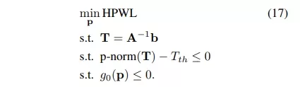
II. Problem statement
We consider a standard package architecture [18], in which chiplets are bonded to the interposer via microbumps, and macrobumps connect the interposer to the package (Fig. 1). The package is secured with soldered bumps. To efficiently dissipate heat, a copper lid and heat sink are included. Heat dissipation is managed using a convective boundary condition applied to the top surface of the heat sink. Thermal interface materials are included between the chiplets and the lid, as well as between the lid and the heat sink. For complex geometries, such as the bumps and interposer, a homogenized anisotropic thermal conductivity is used. The sizes of each layer, along with their thermal conductivity tensors, are reported in Table I. The goal is to minimize the total wirelength while maintaining the maximum temperature below a specified threshold, Tth, and ensuring chiplets do not overlap. To this end, we consider Nc = 8 chiplets (shown in Fig. 1a), including four high-bandwidth memory (H) blocks and four compute (C) blocks. The connections among chiplets are described by the adjacency matrix 𝐀, which is 1 only when chiplet i is connected with chiplet j and zero otherwise (Fig. 2a). Note that connections are intended as unidirectional; thus Aij=1 does not imply that Aji=1. In our example, as illustrated in Fig. 1a, there are 10 connections. Chiplets are assigned a dissipated power, Hi, and dimensions Lix,Liy, where i=0,…,Nc−1 (Fig. 2b); the thickness of each die is fixed (0.25 mm). The positions of the chiplets are denoted by 𝐩 ∈ ℛNc×2, comprising 2Nc degrees of freedom. The total wirelength is estimated by the Half Perimeter Wirelength (HPWL) [19], formulated as [19]
while the temperature map is evaluted by the standarnd heat conduction equation
In Eq. II, the convective heat transfer coefficient is h=3×10³ Wm-2 K-1, the ambient temperature Tamb=20°C, Ω is the simulation domain, Γ1 is the top side of the sink and Γ2 is the remaining of the boundary, which is treated as adiabatic. Equation II is discretized using the finite-volume method, resulting in the following linear system

where 𝐀 ∈ ℛN×N, 𝐓∈ℛN, 𝐛∈ℛN, and N=NxNyNz is the number of control volumes. In this work, the grid is Nx=100,Ny=100 and Nz=222, amounting to 2.22 million degrees of freedom. The higher resolution along the z-axis accounts for the small thickness of layers compared to their in-plane dimensions. The control volume has the dimension 0.8×0.8×0.025 mm3.
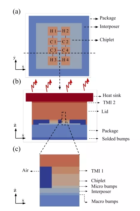
Figure 1:(a). Top view on the chiplet configurations. The connections among chiplets are shown in red. The lid and heat sink are omitted. (b) Vertical cut where the z-dimension is magnified 10x for clarity. (c) Close-up of the chiplet portion of the simulation domain.
| Layer | Thermal Conductivity (κxx, κyy, κzz) [Wm-1K-1] |
Size (Lx, Ly, Lz) [mm] |
|---|---|---|
| Heat Sink | (385,385,385) | (80,80,1) |
| TMI 2 | (1.6,1.6,1.6) | (66,66,0.15) |
| Lid | (385,385,385) | (66,66,2.0) |
| TMI 1 | (1.6,1.6,1.6) | (Lx,Ly,0.15) |
| Chiplet | (150,150,150) | (Lx,Ly,0.25) |
| Micro bumps | (0.9,0.9,2.5) | (Lx,Ly,0.05) |
| Interposer | (128,128,148) | (50,50,0.1) |
| Macro bumps | (0.9,0.9,2.5) | (50,50,0.05) |
| Substrate | (0.33,0.33,0.33) | (66,66,1.5) |
| Solded bumps | (1.2,1.2,2.8) | (66,66,0.3) |
| Air | (0.024,0.024,0.024) | —- |
TABLE I: Size and thermal conductivity tensors of each layer, and for air. The thickness of the lid is 1 mm along all three directions.
| Chiplet | Position (x, y) [mm] |
Size (Lx, Ly) [mm] |
Power H [W] |
|---|---|---|---|
| H 1 | (-7,16) | (10,10) | 20 |
| H 2 | (7,16) | (10,10) | 20 |
| H 3 | (-7,-16) | (10,10) | 20 |
| H 4 | (7,-16) | (10,10) | 20 |
| C 1 | (-7,5) | (10,8) | 30 |
| C 2 | (7,5) | (10,8) | 30 |
| C 3 | (-7,-5) | (10,8) | 30 |
| C 4 | (7,-5) | (10,8) | 30 |
TABLE II: Chiplet layout and properties.
III. Regularization
Equation II needs to be regularized because the maximum and minimum functions are not differentiable. To this end, we use the logsumexp softmax/min functions [19]
with γ=10−3. Using these expressions, the HPWL becomes
To regularize the maximum temperature from Eq. 3, we use the p-norm approximation, which is commonly used in thermal inverse problems [20],
with p = 90. Another term that needs regularization is the heat source H in Eq. II. In fact, assuming spatially uniform power dissipation, each chiplet is assigned a 3D box function, which is not differentiable.
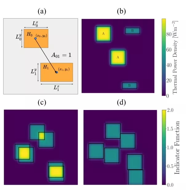
Figure 2:(a) Sketch depicting two connected chiplets and their parameters. (b) Example pf spatial power density distribution associated with a set of chiplets. (c) The initial chiplets configuration for the optimization problem from Eq. 13. (d) The optimized chiplets positions.
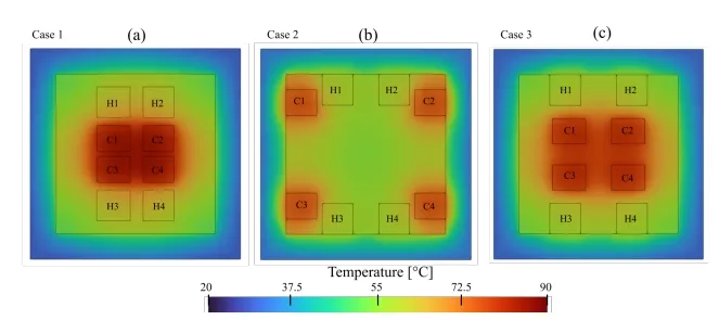
Figure 3:(a) Temperature map for the initial configuration (Case 1), comprising four high-bandwidth and four compute units. The peak temperature is 85.98°C. (b) Temperature distribution for the case where the maximum temperature is minimized without HPWL constraint (Case 2), with a peak of 75.44°C. (c) The configuration that minimizes the HPWL while keeping the temperaturte below 82°C (Case 3). The peak temperature is 80.81°C.
The key idea is to smooth out this box function along the xy plane, while keeping the discontinuity along z, where differentiability is not needed. The first step is to express the heat source as
where ℋ∥ and ℋz, are the in-plane 2D and out-of-plane 2D Heaviside functions. The term zc is the midpoint in the z direction of the chiplets. Next, we regularize the in-plane Heaviside functions with
where α=1 is a smoothing parameter. An example of power dissipation map is shown in Fig. 1-b. A similar regularization approach is applied to the space-dependent thermal conductivity. Specifically, each movable block is composed of a microbump layer, a die and a thermal material interface. Their corresponding thermal conductivity distributions need to be differentiable along the xy-plane. Let’s refer to the thickness, the midpoint in their z direction, and thermal conductivity of each of these three layers as tl, zl and κl, respectively, with l=0,1,2. Then, the space-dependent thermal conductivity is
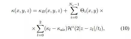
where κB is the thermal conductivity of the fixed part of the simulation domain; as this term also includes the air enclosed by the lid, in Eq. III, we subtract κair from κl.
IV; non-overlap constraint
During optimization, chiplets may overlap; to avoid such a scenario, we introduce an inequality constraint based on the following rationale: Suppose we have a 2D function that is 1 only at the chiplet locations and zero elsewhere, the maximum of such a function becomes larger than one when overlap occurs. To make such a constraint differentiable, we combine two concepts discussed in the last section. First, we build the smooth 2D function
and then compute the maximum value as p-norm(f). The non-inequality constraint is
with p=90. Note that we used the discretized version of f, given by fk=f(xk,yk). To validate this approach, we solve the following optimization problem

Throughout this work, as an optimizer, we choose the Method of Moving Asymptotes (MMA) [21]. The starting guess, shown in Fig. 2-c, is a set of partially overlapped chips. As illustrated in Fig. 2-d after roughly 20 iterations, the chiplets do indeed spread zeroing the overlap.
VResults
We first consider the configuration shown in Fig. 1a, where the regularized (from Eq. II) and the real HPWL are 92 and 103.1 mm, respectively (Tab. IV). We refer to this scenario as “Case 1.” The temperature map, shown in Fig. 3a, is higher in the central area, where the high-power blocks (compute units) are located. The peak value is 85.98°C, while the regularized one, computed by Eq. 7, is 81.20°C. For comparison, we also compute the temperature map with ANSYS, which predicts a temperature peak of 86.85°C, falling within 1% error. Next, to test the optimization algorithm, we minimize the peak temperature while avoiding chiplet overlap (Case 2). The first guess is given by the configuration in Fig. 1a. The optimization algorithm is
As illustrated in Fig. 4a, the real maximum temperature decreases by approximately 10°C over 30 iterations, reaching a peak temperature of 75.44°C. In the final arrangement depicted in Fig. 3b, the chiplets are positioned near the border, with compute units spaced farther apart. This layout is expected, as components with higher power tend to be more susceptible to thermal crosstalk. We note that the final layout maintains the symmetry of the initial guess since the convective boundary condition applied at the top surface is applied uniformly. The regularized temperature, also shown in Fig. 4a, remains consistently lower by about 5°C, closely mirroring the trend of the actual temperature. This observation corroborates the effectiveness of using the p-norm as a representation of the maximum temperature. For this configuration, ANSYS predicts a peak temperature of 76.33°C, which, again, is within 1% error.
Figure 4:(a) The evolution of the p-norm and real maximum temperature for Case 2, where there is no constraint on the HPWL. The two quantities follow the same trend and are consistently about 5°C apart, corroborating the use of the pnorm as a proxy for the maximum temperature (b) The evolution of the non-overlap constraint g0 from Eq. 12. It follows closely its real counterpart.
| Solver |
Case 1
[C°]
|
Case 2
[C°]
|
Case 3
[C°]
|
|---|---|---|---|
| DiffChip (p-norm) | 81.20 | 70.77 | 76.28 |
| DiffChip (real) | 85.98 | 75.44 | 80.81 |
| ANSYS | 86.85 | 76.33 | 81.67 |
TABLE III: Peak Temperatures for different cases.
| HPWL |
Case 1
[mm]
|
Case 2
[mm]
|
Case 3
[mm]
|
|---|---|---|---|
| Softmax | 92 | 203.5 | 120.8 |
| Real | 103.1 | 209.2 | 128.6 |
TABLE IV:The half-permimeter wirelength (HPWL) for different cases.
| Chiplet |
Case 1
(x, y)
[mm]
|
Case 2
(x, y)
[mm]
|
Case 3
(x, y)
[mm]
|
|---|---|---|---|
| H 1 | (-7,16) | (-8.93,20.) | (-10.21,20.) |
| H 2 | (7,16) | (8.93,20.) | (10.21,20) |
| H 3 | (-7,-16) | (-8.93,-20) | (-10.21,-20) |
| H 4 | (7,-16) | (8.93,-20) | (10.21,-20) |
| C 1 | (-7,5) | (-19.9, 15.83) | (-9.07, 6.85) |
| C 2 | (7,5) | (19.9, 15.83) | (9.07, 6.85) |
| C 3 | (-7,-5) | (-19.9 ,-15.83) | (-9.07,-6.85) |
| C 4 | (7,-5) | (19.9 ,-15.83) | (9.07,-6.85) |
TABLE V:Chiplet layout for different cases.
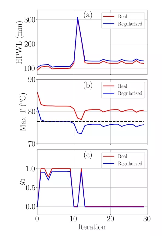
Figure 5:(a) The evolution of the HPWL (both the real and the regularized one). It increases as the optimization progresses in order to accomodate the constraint on the maximum temperature. (b) Trajectory of the maximum temperature. At convergence, the regularized temperature falls below Tth=75°C (c) The evolution of the nonoverlap constraint. After an initial phase, where it is violated, both the real and the regularized constraint approche zero. i.e. the constraint it satisfied.
The evolution of the nonoverlap constraint, as depicted in Fig. 4b, is oscillatory. This indicates that the optimizer can rapidly reposition chiplets to reduce overlap without substantially affecting the cost function. However, this is not the case when minimizing the HPWL, as will be discussed later. Since in this case there is no constraint on the HPWL, its final value is as large as 209.2 mm, with the regularized counterpart being 203.5 mm. Finally, as illustrated in Fig. 4b, the regularized nonoverlap constraint closely matches its nondifferentiable counterparts, achieved by substituting the p-norm with the maximum value in Eq. 12.
As the last example (Case 3), we consider the case where HPWL is minimized while constraining the p-norm temperature below a threshold, and ensuring no overlap. Supposed we want to maintain the peak temperature below 82°C. From Case 2, we noted that there is a gap of about 5°C between the real and regularized peak temperature. Thus, we set Tth = 77°C. The corresponding algorithm reads
Remarkably, this optimization converges in fewer than 15 iterations. The final configuration, depicted in Fig. 3c, maintains the symmetry of the first guess, analogously to Case 2. The optimization finds a balance between two contrasting needs: Minimizing the maximum temperature requires chiplets to be spaced apart, while minimizing the HPWL necessitates closer packing of the dies. This trend is illustrated in Fig. 5a and b, where the HPWL increases and the maximum regularized temperature decreases until it falls below Tth, stabilizing around 76.28°C <Tth. The corresponding real maximum temperature is 80.81°C, which is below the intended target.
The ANSYS’s prediction is within 1% error (81.67°C). The actual HPWL for the final configuration is 128.6 mm, which, as expected, lies between Cases 1 and 2. As depicted in Fig. 5c, the nonoverlap constraint is initially violated due to the need for a low HPWL but eventually falls below zero. This behavior differs from Case 2, where the nonoverlap constraint does not conflict with other requirements. We note that in practical layouts chiplets are packed tighter in order to satisfy electrical constraints, such as data delay [7]. Possible future iterations of DiffChip will include these constraints. Additionally, the orientation of the chiplet can be considered a degree of freedom. Since changing orientation, such as rotating by 90°, is nondifferentiable, regularization will be necessary.
VI. Conclusions
In conclusion, we present DiffChip, a framework for chiplet floorplanning based on automatic differentiation (AD). By integrating a differentiable thermal solver with smooth space-dependent properties such as thermal conductivity and heat sources, we compute the gradients of the cost function with respect to the chiplet positions. Additionally, the maximum temperature and half-perimeter wirelength (HPWL) are made differentiable through regularization. We successfully apply DiffChip to various scenarios, including minimizing the HPWL under maximum temperature and non-overlap constraints. The final layouts are validated against a commercial software. Unlike gradient-free methods, such as simulated annealing, our approach achieves faster convergence and enables large-scale optimization. Lastly, unlike machine learning approaches, DiffChip requires neither training nor a surrogate, as the underlying physical model is inherently differentiable.
Acknowledgment
The authors thank Arvind Kumar from IBM for helpful discussions and support.
References
- [1] G. E. Moore, “Cramming more components onto integrated circuits,” Proceedings of the IEEE, vol. 86, no. 1, pp. 82–85, 1998.
- [2] C. Douglas, “Advanced heterogeneous integration technology trend for cloud and edge,” in 2017 IEEE Electron Devices Technology and Manufacturing Conference (EDTM). IEEE, 2017, pp. 4–5.
- [3] S. S. Iyer, “Heterogeneous integration for performance and scaling,” IEEE Transactions on Components, Packaging and Manufacturing Technology, vol. 6, no. 7, pp. 973–982, 2016.
- [4] Y.-K. Ho and Y.-W. Chang, “Multiple chip planning for chip-interposer codesign,” in Proceedings of the 50th Annual Design Automation Conference, 2013, pp. 1–6.
- [5] K. Skadron, M. R. Stan, W. Huang, S. Velusamy, K. Sankaranarayanan, and D. Tarjan, “Temperature-aware microarchitecture,” ACM SIGARCH Computer Architecture News, vol. 31, no. 2, pp. 2–13, 2003.
- [6] C. Torregiani, B. Vandevelde, H. Oprins, E. Beyne, and I. De Wolf, “Thermal analysis of hot spots in advanced 3d-stacked structures,” in 2009 15th International Workshop on Thermal Investigations of ICs and Systems. IEEE, 2009, pp. 56–60.
- [7] S. Chen, S. Li, Z. Zhuang, S. Zheng, Z. Liang, T.-Y. Ho, B. Yu, and A. L. Sangiovanni-Vincentelli, “Floorplet: Performance-aware floorplan framework for chiplet integration,” IEEE Transactions on Computer-Aided Design of Integrated Circuits and Systems, 2023.
- [8] Z. Zhuang, B. Yu, K.-Y. Chao, and T.-Y. Ho, “Multi-package co-design for chiplet integration,” in Proceedings of the 41st IEEE/ACM International Conference on Computer-Aided Design, 2022, pp. 1–9.
- [9] J.-H. Han, X. Guo, K. Skadron, and M. R. Stan, “From 2.5 d to 3d chiplet systems: Investigation of thermal implications with hotspot 7.0,” in 2022 21st IEEE Intersociety Conference on Thermal and Thermomechanical Phenomena in Electronic Systems (iTherm). IEEE, 2022, pp. 1–6.
- [10] C. Wang, Q. Xu, C. Nie, H. Cao, J. Liu, and Z. Li, “An efficient thermal model of chiplet heterogeneous integration system for steady-state temperature prediction,” Microelectronics Reliability, vol. 146, p. 115006, 2023.
- [11] R. Zhang, M. R. Stan, and K. Skadron, “Hotspot 6.0: Validation, acceleration and extension,” University of Virginia, Tech. Rep, 2015.
- [12] F. Eris, A. Joshi, A. B. Kahng, Y. Ma, S. Mojumder, and T. Zhang, “Leveraging thermally-aware chiplet organization in 2.5 d systems to reclaim dark silicon. in 2018 design, automation & test in europe conference & exhibition (date),” 2018.
- [13] L. Chen, W. Jin, and S. X.-D. Tan, “Fast thermal analysis for chiplet design based on graph convolution networks,” in 2022 27th Asia and South Pacific Design Automation Conference (ASP-DAC). IEEE, 2022, pp. 485–492.
- [14] R. V. Woldseth, N. Aage, J. A. Bærentzen, and O. Sigmund, “On the use of artificial neural networks in topology optimisation,” Structural and Multidisciplinary Optimization, vol. 65, no. 10, p. 294, 2022.
- [15] J. Bradbury, R. Frostig, P. Hawkins, M. J. Johnson, C. Leary, D. Maclaurin, G. Necula, A. Paszke, J. VanderPlas, S. Wanderman-Milne, and Q. Zhang, “JAX: composable transformations of Python+NumPy programs,” 2018. [Online]. Available: http://github.com/google/jax
- [16] G. Romano and S. G. Johnson, “Inverse design in nanoscale heat transport via interpolating interfacial phonon transmission,” Structural and Multidisciplinary Optimization, vol. 65, no. 10, p. 297, 2022.
- [17] A. M. Hammond, A. Oskooi, S. G. Johnson, and S. E. Ralph, “Photonic topology optimization with semiconductor-foundry design-rule constraints,” Optics Express, vol. 29, no. 15, pp. 23 916–23 938, 2021.
- [18] A. Jain, R. Miyazawa, S. Raghavan, P. R. Chowdhury, M. G. Farooq, A. Kumar, and K. Sakuma, “Thermal characterization of 3-d stacked heterogeneous integration (hi) package for high-power computing applications,” in 2023 IEEE 73rd Electronic Components and Technology Conference (ECTC). IEEE, 2023, pp. 1219–1225.
- [19] B. B. Ray, A. R. Tripathy, P. Samal, M. Das, and P. Mallik, “Half-perimeter wirelength model for vlsi analytical placement,” in 2014 International Conference on Information Technology. IEEE, 2014, pp. 287–292.
- [20] D. J. Lohan, E. M. Dede, and J. T. Allison, “A study on practical objectives and constraints for heat conduction topology optimization,” Structural and Multidisciplinary Optimization, vol. 61, no. 2, pp. 475–489, 2020.
- [21] K. Svanberg, “The method of moving asymptotes—a new method for structural optimization,” International journal for numerical methods in engineering, vol. 24, no. 2, pp. 359–373, 1987. [Online]. Available: https://onlinelibrary.wiley.com/doi/abs/10.1002/nme.1620240207
Related Chiplet
- DPIQ Tx PICs
- IMDD Tx PICs
- Near-Packaged Optics (NPO) Chiplet Solution
- High Performance Droplet
- Interconnect Chiplet
Related Technical Papers
- STAMP-2.5D: Structural and Thermal Aware Methodology for Placement in 2.5D Integration
- Exploring the Efficiency of 3D-Stacked AI Chip Architecture for LLM Inference with Voxel
- Intel Delivers Cutting-Edge Process Technologies to the Data Center with Intel 18A and Advanced Chiplet Packaging
- Chiplet-Gym: Optimizing Chiplet-based AI Accelerator Design with Reinforcement Learning
Latest Technical Papers
- Affinity Tailor: Dynamic Locality-Aware Scheduling at Scale
- AMMA: A Multi-Chiplet Memory-Centric Architecture for Low-Latency 1M Context Attention Serving
- Exploring the Efficiency of 3D-Stacked AI Chip Architecture for LLM Inference with Voxel
- Epoxy Composites Reinforced with Long Al₂O₃ Nanowires for Enhanced Thermal Management in Advanced Semiconductor Packaging
- Chipmunq: A Fault-Tolerant Compiler for Chiplet Quantum Architectures