3D integration of pixel readout chips using Through-Silicon-Vias
Francisco Piernas Diaz 𝑎, Jerome Alozy 𝑎, Sara Al-Tawil 𝑎 , Jan Buytaert 𝑎, Michael Campbell 𝑎, Thomas Fritzsch 𝑏, Kostas Kloukinas 𝑎, Mark Istvan Kovacs 𝑎, Xavier Llopart Cudie 𝑎, Mateus Vicente Barreto Pinto 𝑐 and Ken Wyllie 𝑎
𝑎 European Organization for Nuclear Research (CERN), Geneva, Switzerland
𝑏 IZM Fraunhofer, Berlin, Germany
𝑐 University of Geneva, Geneva, Switzerland
Abstract
Particle tracking and imaging detectors are becoming increasingly complex, driven by demands for densely integrated functionality and maximal sensitive area. These challenging requirements can be met using 3D interconnect techniques widely used in industry. In this paper, we present the results of an evaluation of the 3D Through-Silicon-Via (TSV) technology, using the Timepix4 integrated circuit as a test-vehicle. We will present the concepts for 3D integration and test results from TSV-processed chips bonded to custom-designed circuit boards conceived as proofs-of-principle for future detector modules.
1. Introduction
The evolving demands on solid-state particle-tracking and imaging detectors incorporating pixelated readout application specific integrated circuits (ASIC) require new approaches for power and signal connections. Future systems will provide complex functionality such as timing the hits of particles to the order of tens of picoseconds, as well as precise position and energy measurements. The corresponding needs to deliver clean power to the ASIC circuitry and support high data bandwidths are challenging with traditional interconnect technologies such as wire-bonding. Additionally, space reserved for the interconnects often limits the sensitive area. These concerns have motivated this study into alternative interconnect technologies.
One of these alternatives is the Through-Silicon-Via (TSV), an interconnect that allows access to the active circuitry from the back side of the ASIC, as shown in figure 1. Parasitic effects are lower with TSVs[1], whichimproves signal and power integrity. Furthermore, with TSVs, it is possible to design a pixel detector ASIC without wirebond pads. This minimizes the dead area and allows 4-side buttability.
In order to explore TSV technology, Timepix4 [2] was used as a test vehicle. This is a read-out ASIC with wirebond and Ball-Grid-Array (BGA) dicing options, designed to be flip-chip bonded with a silicon sensor to form a hybrid pixel detector. It covers almost 7cm2 of sensitive area and has 16 output links, with a bandwidth limited to 1.25Gbps in the version of the ASIC used for this study. The connections of the ASIC are distributed in three peripheries (Top, Center and Bottom) with the Center accessible only with TSVs and Top/Bottom with TSVs or bond wires. TSV processing of this ASIC involved creating the TSVs, routing the signals from the TSVs to BGA pads on the back surface of the die, by using a Redistribution Layer (RDL), and finally dicing off the wirebond pads.
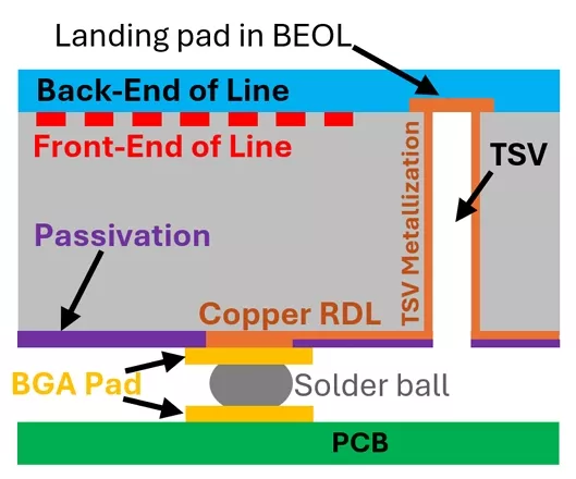
Figure 1: Diagram (not to scale) showing how a TSV connects an internal landing pad in the Back-end of Line (BEOL) of the ASIC to a PCB.
2. TSV processing of Timepix4
TSVs are fabricated by Deep Reactive Ion Etching (DRIE) following the so-called BOSCH process [3]. They can be processed at three different stages of wafer manufacturing, and are hence referred to as TSV-First, TSV-Middle or TSV-Last [1]. TSV-Last involves the post-processing of completed ASIC wafers and was the only possible approach for this study
TSV-Last processing of Timepix4 was done by IZM Fraunhofer. Wafers were first thinned down to 120μm, then etching of the silicon began from the back side of the wafer. The alternative of etching from the front-side would require ‘keep-out’ zones for the TSV processing, which contributes to the dead-area. After oxide-passivation of the TSV-side walls, the passivation was opened at the bottom of the via to allow an electrical connection to the TSV landing pads in the first layers of the BEOL-stack of Timepix4. Then the TSVs were metallized and the RDL deposited by copper electroplating. The resulting TSV structure is shown in figure 2.

Figure 2: Scanning-electron-microscope picture of a TSV in Timepix4, after cross-sectioning by a Focused Ion Beam. The front-side flip-chip bonding pads are used to connect to a silicon sensor.
Three rows of 147 TSVs (with nominal diameter 55μm), connecting to the three peripheries of the ASIC, were fabricated. A copper RDL distributes the signals and power nets across the back surface of the ASIC to 1020 BGA pads, each of 300μm in diameter and a pitch of 800μm. Figure 3 shows the back side of the ASIC after TSV processing.
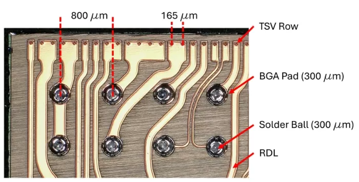
Figure 3: Timepix4-TSV back side, showing a row of TSVs, BGA pads and RDL. This particular sample also has solder balls, deposited on the BGA pads
3. Results with Test-Socket PCB
Aprinted circuit board was designed for testing Timepix4-TSV using a custom-manufactured socket (figure 4). The solderless socket consists of an array of pogo-pins matching the BGA pads on the ASIC. The pins were proven to make good contact to the bare BGA pads, so ASIC testing was possible even before balling the BGA. This PCB was used to identify faulty ASICs and testing working ones. It is also compatible with direct assembly of ASICs without mounting the socket, either by Anisotropic Conducting Paste (ACP) or solder balls as shown in figure 4 and 5.
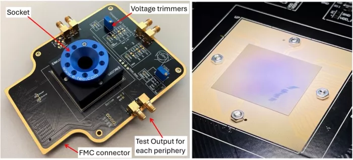
Figure 4: Left: Test-Socket PCB with adjustable voltage to power the ASIC, bottom side FMC connector to interface to the controller board and SMA connectors for testing. Right: same PCB without socket and a Timepix4-TSV bonded with ACP glue.
Results with first batch. Processing of this batch was affected by technical problems with the equipment. The final yield was low, with one of the two wafers fully faulty. Some ASICs of both wafers had the wirebond pads intentionally not diced off. This allowed direct comparison between the resistance for some power nets, measured on the wirebond pads which are internally connected in the ASIC compared to measuring on BGA pads. Overall a higher resistance was found on BGA pads for the faulty wafer, sometimes by two orders of magnitude. Taking into account that the landing pad of the TSV is shorted with the wirebond pads, a possible explanation is a poor connection between the TSVs and the landing pads.
Results with second batch. In this batch the yield was higher, 94% with a total of 48 out of 51 working ASICs. Two ASICs failed to work and one had defective columns of pixels (not related to TSV processing). The working samples were fully characterized, including noise and threshold measurements. Their performance was identical to Timepix4 ASICs without TSVs, proving that there was no degradation due to the wafer post-processing.
Samples of working ASICs were selected to test two alternative methods for connecting the ASIC to a substrate. The first was by depositing solder balls on the BGA pads (figure 5 left), and then reflow soldering the ASIC to substrates. The balling of the ASICs was performed by PacTech [4], using SAC305 alloy solder balls of 300 μm. The second method used ACP, consisting of small conducting particles mixed with glue (figure 5 right). This mixture creates the connection between the pads on the ASIC and the pads on the substrate. Additionally, samples were sent to Advafab [6] for sensor bonding trials. Figure 6 shows a sample of Timepix4-TSV with sensor and the result of exposure to a radioactive beta source, tested with the socket module, which indicated that the chip is fully functional with TSVs and sensor bonded
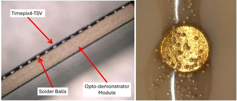
Figure 5: Two methods of bonding an ASIC to PCB: balling the ASIC and soldering (left) or bonding with ACPglue (right) using 30 μm metal particles deposited on the opto-demonstrator module (section 4)
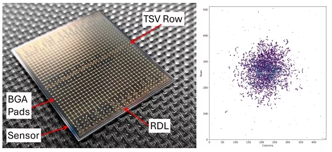
Figure 6: Left: Timepix4-TSV back-side, with sensor. Right: result of exposure to Strontium-90
4. Results with opto-demonstrator module
The concept for this module is a proof of principle for future particle detectors, where a front-end ASIC is connected via TSVs and sends data to an opto-electronic transmitter. A 2-side buttable PCB was designed to implement this idea. It uses a Timepix4-TSV (bonded by ACP glue or solder balls) and four VTRx+ [5] modules, each with four optical transmitter channels. This was a challenging design due to the dense routing and signal integrity requirements of the 16 output channels. Power distribution to the ASIC was optimized using layout techniques, as shown in figure 7. Copper cutouts in the power plane were used to guide the current flow and ensure a more uniform voltage drop on the pads of the ASIC. An assembly of this PCB with a Timepix4-TSV, bonded with solder balls was tested. Figure 8 shows the eye diagram for one link at 1.25Gbps through optical fiber, indicating good transmission of a pseudo-random data pattern through TSV, substrate stripline and optical fiber. This result demonstrates the feasibility of such an assembly with BGA balls and TSVs.
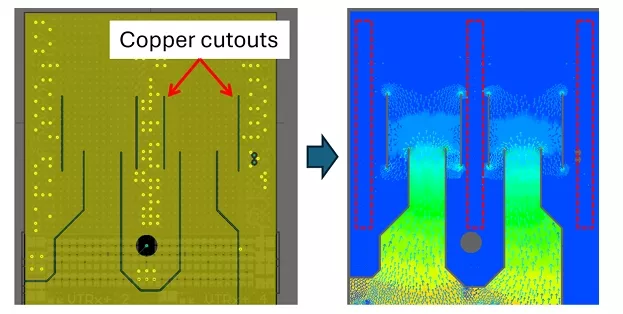
Figure 7: Simulated copper cutouts in the power plane of the module, to distribute current flow and make the voltage drop more uniform. Blue color indicates higher static voltage drop (30mV) which is uniform in the location of the power pads, indicated by the dashed red rectangles
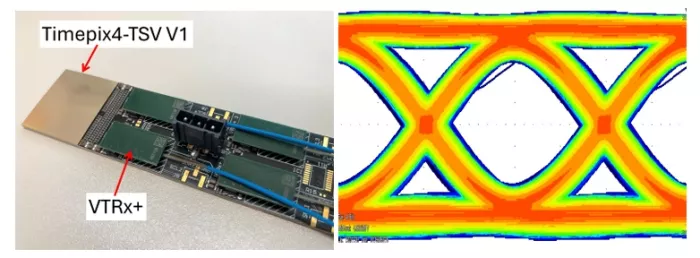
Figure 8: Left: opto-demonstrator module, showing a Timepix4-TSV soldered with BGA balls and four VTRx+ modules. Right: eye diagram produced with a pseudo-random bit sequence using one of the 16 channels, through TSV and optical fiber at 1.25Gbps.
5. Conclusion
Thefeasibility of connecting Timepix4 ASICs with TSVs has been investigated. TSVs were successfully fabricated using a TSV-Last process. Two modules were designed to test the ASICs: a socket PCB and a 2-side buttable opto-demonstrator using VTRx+ for conversion of the data links to optical f iber. Our results indicate that the interconnections through TSVs are successfully delivering power and transmitting data to and from the ASIC. At the moment of writing, three wafers of a higher bandwidth version of Timepix4 are being TSV processed. This will allow testing of data transmission through TSVs at 5.12Gbps.
Acknowledgments
The presented work was supported by the Medipix4 collaboration and the CERN EP R&D WP 5.
References
[1] T. Fritzsch et al., 3D TSV hybrid pixel detector modules with ATLAS FE-I4 readout electronic chip, 2022 JINST 17 C01029.
[2] X. Llopart et al., Timepix4, a large area pixel detector readout chip which can be tiled on 4 sides providing sub-200 ps timestamp binning, 2022 JINST 17 C01044.
[3] F. Laerme, A. Schilp, K. Funk and M. Offenberg, Bosch deep silicon etching: improving uniformity and etch rate for advanced MEMS applications, in the proceedings of the Technical Digest. IEEE International MEMS99Conference. Twelfth IEEE International Conference on Micro Electro Mechanical Systems (Cat. No.99CH36291), Orlando, FL, U.S.A. (1999), p. 211–216 [DOI:10.1109/memsys.1999.746812].
[4] PacTech — Packaging Technologies GmbH, https://pactech.com.
[5] J. Troska et al., The VTRx+, an optical link module for data transmission at HL-LHC, PoS TWEPP-17 (2017) 048.
[6] ADVAFABOY, https://advafab.com.
Related Chiplet
- DPIQ Tx PICs
- IMDD Tx PICs
- Near-Packaged Optics (NPO) Chiplet Solution
- High Performance Droplet
- Interconnect Chiplet
Related Technical Papers
- Die-Level Transformation of 2D Shuttle Chips into 3D-IC for Advanced Rapid Prototyping using Meta Bonding
- System-Technology Co-Optimization for Dense Edge Architectures using 3D Integration and Non-Volatile Memory
- Co-Optimization of Power Delivery Network Design for 3-D Heterogeneous Integration of RRAM-Based Compute In-Memory Accelerators
- A3D-MoE: Acceleration of Large Language Models with Mixture of Experts via 3D Heterogeneous Integration
Latest Technical Papers
- Link Quality Aware Pathfinding for Chiplet Interconnects
- Effects of Poor Workload Partitioning on System Performance for Chiplet-Based Systems
- Mozart: Modularized and Efficient MoE Training on 3.5D Wafer-Scale Chiplet Architectures
- Network Design for Wafer-Scale Systems with Wafer-on-Wafer Hybrid Bonding
- CarbonPATH: Carbon-aware pathfinding and architecture optimization for chiplet-based AI systems