IEEE Study Achieves Efficient Integration of Quantum Dot Lasers on Silicon Chiplets
Researchers have developed a novel method for integrating quantum dot laser within silicon for scalable photonics
PISCATAWAY, N.J. -- July 10, 2025 -- III-V semiconductor lasers can be monolithically integrated with photonic chips by directly growing a crystalline layer of laser material, such as indium arsenide, on silicon substrate. However, photonic chips with such integrated laser source are challenging to manufacture due to mismatch between structures or properties of III-V semiconductor material and silicon.
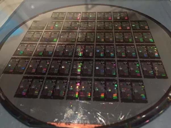
Researchers have now developed an efficient technique for integrating quantum dot lasers within silicon chiplets.
In a study that was recently published in the IEEE Journal of Lightwave Technology, Dr. Rosalyn Koscica from the University of California, United States, and her team successfully integrated indium arsenide quantum dot (QD) lasers monolithically on silicon photonics chiplets. According to Dr. Koscica, "Photonic integrated circuit applications call for on-chip light sources with a small device footprint to permit denser component integration."
To achieve this monolithic integration, the authors combined three key concepts: the pocket laser strategy for monolithic integration, a two-step material growth scheme that includes both metalorganic chemical vapor deposition and MBE for a smaller initial gap size, and a polymer gap-fill approach to minimize optical beam divergence in the gap.
On testing, the chiplets with monolithically integrated lasers demonstrated sufficiently low coupling loss. As a result, the QD lasers operate efficiently on a single O-band wavelength within chiplets. The O-band wavelength is desirable as it allows for transmission of signals within photonic devices with low dispersion. Lasing in the single frequency is achieved using ring resonators made from silicon or distributed Bragg reflectors made from silicon nitride.
"Our integrated QD lasers demonstrated a high temperature lasing up to 105 °C and a life span of 6.2 years while operating at a temperature of 35 °C," says Dr. Koscica.
The proposed integration technique can be applied to a variety of photonic integrated circuit designs, paving the way for a scalable, cost-effective monolithic integration of on-chip light sources for practical applications.
Reference
Title of original paper: Quantum Dot DBR Lasers Monolithically Integrated on Silicon Photonics by In-Pocket Heteroepitaxy
Journal: IEEE Journal of Lightwave Technology
Related Chiplet
- Interconnect Chiplet
- 12nm EURYTION RFK1 - UCIe SP based Ka-Ku Band Chiplet Transceiver
- Bridglets
- Automotive AI Accelerator
- Direct Chiplet Interface
Related News
- DreamBig Semiconductor Announces Partnership with Samsung Foundry to Launch Chiplets for World Leading MARS Chiplet Platform on 4nm FinFET Process Technology Featuring 3D HBM Integration to Solve Scale-up and Scale-out Limitations of AI for the Masses
- OKI Develops Tiling crystal film bonding (CFB) Technology for Heterogeneous Integration of Optical Semiconductors onto 300 mm Silicon Wafers
- Chiplets to quantum: Joe Barry on Analog’s disruptive future
- Automotive Meets Chiplets: Robert Bielby’s Perspective on the Impact of Level 3 ADAS on Emerging Semiconductor Tech
Latest News
- Qualcomm Completes Acquisition of Alphawave Semi
- Cadence Tapes Out UCIe IP Solution at 64G Speeds on TSMC N3P Technology
- Avnet ASIC and Bar-Ilan University Launch Innovation Center for Next Generation Chiplets
- SEMIFIVE Strengthens AI ASIC Market Position Through IPO “Targeting Global Markets with Advanced-nodes, Large-Die Designs, and 3D-IC Technologies”
- FormFactor Expands Silicon Photonics Test Capabilities With Acquisition of Keystone Photonics