Are ghiplets the next evolution stage in GPU designs?
By Majeed Ahmad, EDN (April 1, 2024)

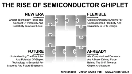
 When GPUs are implemented in a chiplet arrangement, can they be called ghiplets? Semiconductor industry professional Chetan Arvind Patil thinks so. In his blog “The Rise of Semiconductor Ghiplet”, Patil outlines the benefits of GPUs in chiplet architectures compared to monolithic GPU designs currently struggling with lower yield rates for large and complex GPU devices.
In other words, all the rendering is handled by chiplets instead of a big-compute GPU. Take the case of AMD’s Radeon RX 7000 series, one of the first chiplet-based GPUs, which incorporates a large graphics die and several memory dies. The Silicon Valley-based semiconductor firm is now considering using even more chiplets in a GPU design.
To read the full article, click here
Related Chiplet
- DPIQ Tx PICs
- IMDD Tx PICs
- Near-Packaged Optics (NPO) Chiplet Solution
- High Performance Droplet
- Interconnect Chiplet
Related News
- New AMD Patent Describes Potential Chiplet-Based GPU Design
- How to Build a Better “Blackwell” GPU Than Nvidia Did
- Safety architecture boosts automotive GPU for chiplets
- Intel patents chiplet GPU design
Latest News
- Wooptix Targets AI Packaging Bottleneck with Astronomy Tech
- Kenyi Technologies to collaborate with ADTechnology to co-develop a Server Processor targeting Edge AI and Telco use cases
- Tawazun and Lockheed Martin Sign Strategic Agreement to Establish UAE's Chiplet Design and Assembly Facility
- Xanadu and EV Group partner to build industrial-scale photonic quantum hardware
- AI Optical Interconnect Boom Drives U.S. Firms to Expand Southeast Asia Outsourcing, Opening the Door for Cross-Industry Entrants