Chiplets diary: Three anecdotes recount design progress
By Majeed Ahmad, EDN (February 2, 2024)
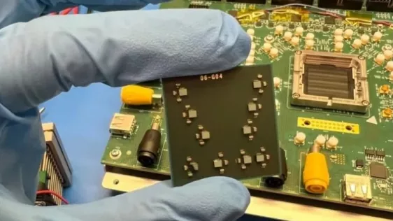
By The chiplet design movement representing multi-billion-dollar market potential is marching ahead with key building blocks falling in place while being taped out at advanced process nodes like TSMC’s 3 nm. These multi-die packaging devices can now mix and match pre-built or customized compute, memory, and I/O ingredients in different process nodes, paving the way for system-in-packages (SiPs) to become the system motherboard of the future.
Chiplets also promise considerable cost reduction and improved yields compared to traditional system-on-chip (SoC) designs. Transparency Market Research forecasts the chiplet market to reach more than $47 billion by 2031, becoming one of the fastest-growing segments of the semiconductor industry at more than 40% CAGR from 2021 to 2031.
Below are a few anecdotes demonstrating how chiplet-enabled silicon platforms are making strides in areas such as packaging, memory bandwidth, and application-optimized IP subsystems.
To read the full article, click here
Related Chiplet
- Interconnect Chiplet
- 12nm EURYTION RFK1 - UCIe SP based Ka-Ku Band Chiplet Transceiver
- Bridglets
- Automotive AI Accelerator
- Direct Chiplet Interface
Related News
- Why chiplets will transform electronic system design
- Chiplets drive new automated design tools at Leti
- Chiplets Make Progress Using Interconnects As Glue
- Chiplets: Revolutionizing Semiconductor Design and Manufacturing
Latest News
- Where co-packaged optics (CPO) technology stands in 2026
- Qualcomm Completes Acquisition of Alphawave Semi
- Cadence Tapes Out UCIe IP Solution at 64G Speeds on TSMC N3P Technology
- Avnet ASIC and Bar-Ilan University Launch Innovation Center for Next Generation Chiplets
- SEMIFIVE Strengthens AI ASIC Market Position Through IPO “Targeting Global Markets with Advanced-nodes, Large-Die Designs, and 3D-IC Technologies”